

LM4910
SNAS151G – MAY 2004 – REVISED MARCH 2007
www.ti.com
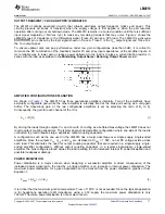
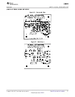
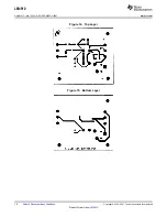
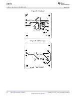
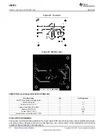
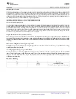
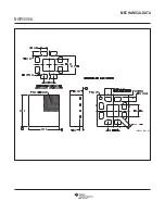
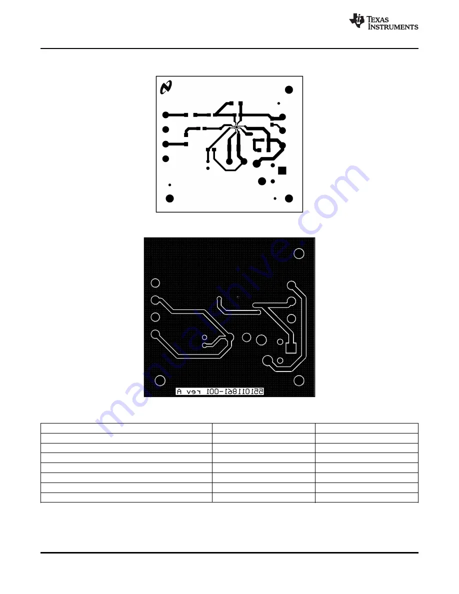
Figure 22. Top Layer
Figure 23. Bottom Layer
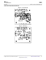
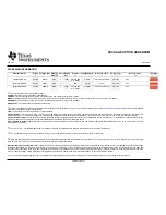
LM4910 Reference Design Boards Bill of Materials
Part Description
Qty
Ref Designator
LM4910 Mono Reference Design Board
1
LM4910 Audio AMP
1
U1
Tantalum Cap 1µF 16V 10
1
Cs
Ceramic Cap 0.39µF 50V Z50 20
2
Ci
Resistor 20k
Ω
1/10W 5
4
Ri, Rf
Resistor 100k
Ω
1/10W 5
1
Rpu
Jumper Header Vertical Mount 2X1, 0.100
1
J1
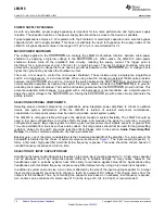
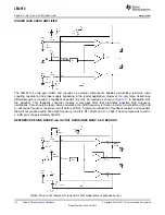
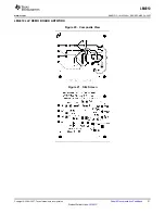
PCB LAYOUT GUIDELINES
This section provides practical guidelines for mixed signal PCB layout that involves various digital/analog power
and ground traces. Designers should note that these are only "rule-of-thumb" recommendations and the actual
results will depend heavily on the final layout.
22
Submit Documentation Feedback
Copyright © 2004–2007, Texas Instruments Incorporated
Product Folder Links:
LM4910


