LM4910
SNAS151G – MAY 2004 – REVISED MARCH 2007
www.ti.com
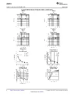
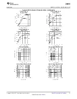
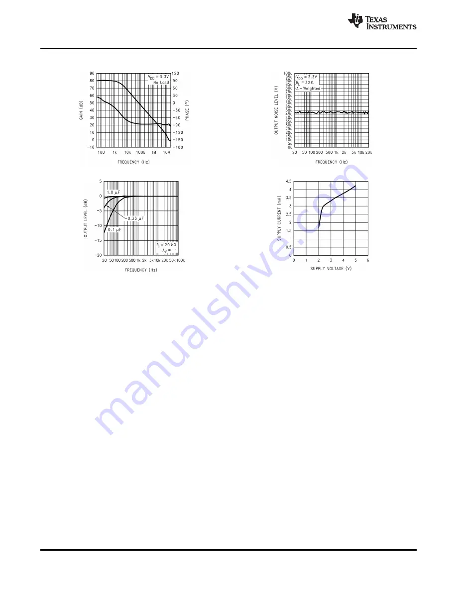
Typical Performance Characteristics (continued)
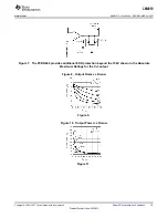
Open Loop Frequency Response
Noise Floor
Frequency Response vs
Supply Current vs
Input Capacitor Size
Supply Voltage
Application Information
ELIMINATING OUTPUT COUPLING CAPACITORS
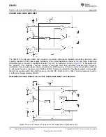
Typical single-supply audio amplifiers that drive single-ended (SE) headphones use a coupling capacitor on each
SE output. This output coupling capacitor blocks the half-supply voltage to which the output amplifiers are
typically biased and couples the audio signal to the headphones. The signal return to circuit ground is through
the headphone jack's sleeve.
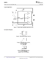
The LM4910 eliminates these output coupling capacitors. Amp3 is internally configured to apply a bandgap
referenced voltage (V
REF
= 1.58V) to a stereo headphone jack's sleeve. This voltage matches the quiescent
voltage present on the Amp1 and Amp2 outputs that drive the headphones. The headphones operate in a
manner similar to a bridge-tied-load (BTL). The same DC voltage is applied to both headphone speaker
terminals. This results in no net DC current flow through the speaker. AC current flows through a headphone
speaker as an audio signal's output amplitude increases on the speaker's terminal.
The headphone jack's sleeve is not connected to circuit ground. Using the headphone output jack as a line-level
output will place the LM4910's bandgap referenced voltage on a plug's sleeve connection. This presents no
difficulty when the external equipment uses capacitively coupled inputs. For the very small minority of equipment
that is DC-coupled, the LM4910 monitors the current supplied by the amplifier that drives the headphone jack's
sleeve. If this current exceeds 500mA
PK
, the amplifier is shutdown, protecting the LM4910 and the external
equipment.
ELIMINATING THE HALF-SUPPLY BYPASS CAPACITOR
Typical single-supply audio amplifers are normally biased to 1/2V
DD
in order to maximize the output swing of the
audio signal. This is usually achieved with a simple resistor divider network from V
DD
to ground that provides the
proper bias voltage to the amplifier. However, this scheme requires the use of a half-supply bypass capacitor to
improve the bias voltage's stability and the amplifier's PSRR performance.
The LM4910 utilizes an internally generated, buffered bandgap reference voltage as the amplifier's bias voltage.
This bandgap reference voltage is not a direct function of V
DD
and therefore is less susceptible to noise or ripple
on the power supply line. This allows for the LM4910 to have a stable bias voltage and excellent PSRR
performance even without a half-supply bypass capacitor.
10
Submit Documentation Feedback
Copyright © 2004–2007, Texas Instruments Incorporated
Product Folder Links:
LM4910


