background image

LM4910

www.ti.com

SNAS151G – MAY 2004 – REVISED MARCH 2007

LM4910

Output Capacitor-less Stereo 35mW Headphone

Amplifier

Check for Samples:

LM4910

1

FEATURES

Available in space-saving MSOP, LLP, and
SOIC packages

2

Eliminates headphone amplifier output
coupling capacitors

APPLICATIONS

Eliminates half-supply bypass capacitor

Mobile Phones

Advanced pop & click circuitry eliminates

PDAs

noises during turn-on and turn-off

Portable electronics devices

Ultra-low current shutdown mode

Portable MP3 players

Unity-gain stable

2.2V - 5.5V operation

DESCRIPTION

The LM4910 is an audio power amplifier primarily designed for headphone applications in portable device
applications. It is capable of delivering 35mW of continuous average power to a 32

load with less than 1%

distortion (THD+N) from a 3.3V

DC

power supply.

The LM4910 utilizes a new circuit topology that eliminates output coupling capacitors and half-supply bypass
capacitors. The LM4910 contains advanced pop & click circuitry which eliminates noises caused by transients
that would otherwise occur during turn-on and turn-off.

Boomer audio power amplifiers were designed specifically to provide high quality output power with a minimal
amount of external components. Since the LM4910 does not require any output coupling capacitors, half-supply
bypass capacitors, or bootstrap capacitors, it is ideally suited for low-power portable applications where minimal
space and power consumption are primary requirements.

The LM4910 features a low-power consumption shutdown mode, activated by driving the shutdown pin with logic
low. Additionally, the LM4910 features an internal thermal shutdown protection mechanism. The LM4910 is also
unity-gain stable and can be configured by external gain-setting resistors.

Table 1. Key Specifications

VALUE

UNIT

PSRR at f = 217Hz

65

dB (typ)

Power Output at V

DD

= 3.3V, R

L

= 32

, and THD

1%

35

mW (typ)

Shutdown Current

0.1

µA (typ)

1

Please be aware that an important notice concerning availability, standard warranty, and use in critical applications of
Texas Instruments semiconductor products and disclaimers thereto appears at the end of this data sheet.

2

All trademarks are the property of their respective owners.

PRODUCTION DATA information is current as of publication date.

Copyright © 2004–2007, Texas Instruments Incorporated

Products conform to specifications per the terms of the Texas
Instruments standard warranty. Production processing does not
necessarily include testing of all parameters.

Summary of Contents for LM4910 Boomer

Page 1: ... to provide high quality output power with a minimal amount of external components Since the LM4910 does not require any output coupling capacitors half supply bypass capacitors or bootstrap capacitors it is ideally suited for low power portable applications where minimal space and power consumption are primary requirements The LM4910 features a low power consumption shutdown mode activated by dri...

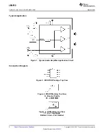
Page 2: ...ication Circuit Connection Diagram Figure 2 MSOP SO Package Top View Figure 3 MSOP Marking Top View G Boomer Family C2 LM4910MM Figure 4 SO Marking Top View TT Die Traceability Bottom 2 lines Part Number 2 Submit Documentation Feedback Copyright 2004 2007 Texas Instruments Incorporated Product Folder Links LM4910 ...

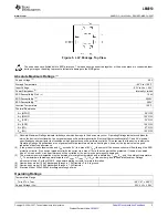
Page 3: ...in the Operating Ratings Specifications are not guaranteed for parameters where no limit is given however the typical value is a good indication of device performance 2 If the product is in shutdown mode and VDD exceeds 6V to a max of 8V VDD then most of the excess current will flow through the ESD protection circuits If the source impedance limits the current to a max of 10ma then the part will b...

Page 4: ...red with respect to the GND pin unless otherwise specified 2 Absolute Maximum Ratings indicate limits beyond which damage to the device may occur Operating Ratings indicate conditions for which the device is functional but do not guarantee specific performance limits Electrical Characteristics state DC and AC electrical specifications under particular test conditions which guarantee specific perfo...

Page 5: ...d with respect to the GND pin unless otherwise specified 2 Absolute Maximum Ratings indicate limits beyond which damage to the device may occur Operating Ratings indicate conditions for which the device is functional but do not guarantee specific performance limits Electrical Characteristics state DC and AC electrical specifications under particular test conditions which guarantee specific perform...

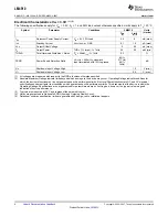
Page 6: ...device is within the Operating Ratings Specifications are not guaranteed for parameters where no limit is given however the typical value is a good indication of device performance 3 Typicals are measured at 25 C and represent the parametric norm 4 Limits are guaranteed to National s AOQL Average Outgoing Quality Level 5 Datasheet min max specification limits are guaranteed by design test or stati...

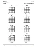
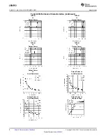
Page 7: ...acteristics THD N THD N vs vs Frequency Frequency THD N THD N vs vs Frequency Frequency THD N THD N vs vs Frequency Frequency THD N THD N vs vs Output Power Output Power Copyright 2004 2007 Texas Instruments Incorporated Submit Documentation Feedback 7 Product Folder Links LM4910 ...

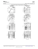
Page 8: ... vs vs Output Power Output Power THD N THD N vs vs Output Power Output Power Output Power vs Output Power vs Load Resistance Load Resistance Output Power vs Output Power vs Load Resistance Supply Voltage 8 Submit Documentation Feedback Copyright 2004 2007 Texas Instruments Incorporated Product Folder Links LM4910 ...

Page 9: ...issipation vs Supply Voltage Output Power Power Dissipation vs Power Dissipation vs Output Power Output Power Channel Separation Power Supply Rejection Ratio Power Supply Rejection Ratio Power Supply Rejection Ratio Copyright 2004 2007 Texas Instruments Incorporated Submit Documentation Feedback 9 Product Folder Links LM4910 ...

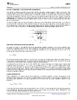
Page 10: ...nected to circuit ground Using the headphone output jack as a line level output will place the LM4910 s bandgap referenced voltage on a plug s sleeve connection This presents no difficulty when the external equipment uses capacitively coupled inputs For the very small minority of equipment that is DC coupled the LM4910 monitors the current supplied by the amplifier that drives the headphone jack s...

Page 11: ...electing the ratio of Rf to Ri Consequently the gain for each channel of the IC is AV Rf Ri 1 By driving the loads through outputs VO1 and VO2 with VO3 acting as a buffered bias voltage the LM4910 does not require output coupling capacitors The typical single ended amplifier configuration where one side of the load is connected to ground requires large expensive output coupling capacitors A config...

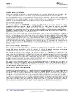
Page 12: ...ions using integrated power amplifiers is critical to optimize device and system performance While the LM4910 is tolerant of external component combinations consideration to component values must be used to maximize overall system quality The LM4910 is unity gain stable which gives the designer maximum system flexibility The LM4910 should be used in low gain configurations to minimize THD N values...

Page 13: ... LM4910 to reproduce peaks in excess of 30mW without producing audible distortion At this time the designer must make sure that the power supply choice along with the output impedance does no violate the conditions explained in the Power Dissipation section Once the power dissipation equations have been addressed the required differential gain can be determined from Equation 2 3 From Equation 2 th...

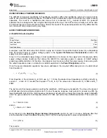
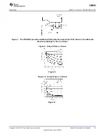
Page 14: ...d to the load by the factor RL RL RSERIES 2 However this may not pose a problem since most headphone applications require less than 10mW of output power Figure 9 illustrates output power 1 THD N vs RSERIES for different loads Figure 7 shows an optional resistor connected between the amplifier output that drives the headphone jack sleeve and ground This resistor provides a ground path that supresse...

Page 15: ...ional ESD protection beyond the 10kV shown in the Absolute Maximum Ratings for the Vo3 output Figure 8 Output Noise vs RSERIES Figure 9 Figure 10 Output Power vs RSERIES Figure 11 Copyright 2004 2007 Texas Instruments Incorporated Submit Documentation Feedback 15 Product Folder Links LM4910 ...

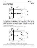
Page 16: ...pass filter that eliminates possible high frequency oscillations Care should be taken when calculating the 3dB frequency in that an incorrect combination of Rf and Cf will cause frequency response roll off before 20kHz A typical combination of feedback resistor and capacitor that will not produce audio band high frequency roll off is Rf 20kΩ and Cf 25pF These components result in a 3dB point of ap...

Page 17: ...AS151G MAY 2004 REVISED MARCH 2007 LM4910 SO DEMO BOARD ARTWORK Figure 12 Composite View Figure 13 Silk Screen Copyright 2004 2007 Texas Instruments Incorporated Submit Documentation Feedback 17 Product Folder Links LM4910 ...

Page 18: ...10 SNAS151G MAY 2004 REVISED MARCH 2007 www ti com Figure 14 Top Layer Figure 15 Bottom Layer 18 Submit Documentation Feedback Copyright 2004 2007 Texas Instruments Incorporated Product Folder Links LM4910 ...

Page 19: ...S151G MAY 2004 REVISED MARCH 2007 LM4910 MSOP DEMO BOARD ARTWORK Figure 16 Composite View Figure 17 Silk Screen Copyright 2004 2007 Texas Instruments Incorporated Submit Documentation Feedback 19 Product Folder Links LM4910 ...

Page 20: ...10 SNAS151G MAY 2004 REVISED MARCH 2007 www ti com Figure 18 Top Layer Figure 19 Bottom Layer 20 Submit Documentation Feedback Copyright 2004 2007 Texas Instruments Incorporated Product Folder Links LM4910 ...

Page 21: ...S151G MAY 2004 REVISED MARCH 2007 LM4910 LLP DEMO BOARD ARTWORK Figure 20 Composite View Figure 21 Silk Screen Copyright 2004 2007 Texas Instruments Incorporated Submit Documentation Feedback 21 Product Folder Links LM4910 ...

Page 22: ...i Resistor 20kΩ 1 10W 5 4 Ri Rf Resistor 100kΩ 1 10W 5 1 Rpu Jumper Header Vertical Mount 2X1 0 100 1 J1 PCB LAYOUT GUIDELINES This section provides practical guidelines for mixed signal PCB layout that involves various digital analog power and ground traces Designers should note that these are only rule of thumb recommendations and the actual results will depend heavily on the final layout 22 Sub...

Page 23: ...a greater amount of design time but will not increase the final price of the board The only extra parts required may be some jumpers Single Point Power Ground Connections The analog power traces should be connected to the digital traces through a single point link A PI filter can be helpful in minimizing high frequency noise coupling between the analog and digital sections Further place digital an...

Page 24: ...xemption for either 1 lead based flip chip solder bumps used between the die and package or 2 lead based die adhesive used between the die and leadframe The component is otherwise considered Pb Free RoHS compatible as defined above Green RoHS no Sb Br TI defines Green to mean Pb Free RoHS compatible and free of Bromine Br and Antimony Sb based flame retardants Br or Sb do not exceed 0 1 by weight ...

Page 25: ...PACKAGE OPTION ADDENDUM www ti com 9 Aug 2013 Addendum Page 2 ...

Page 26: ...Pins SPQ Reel Diameter mm Reel Width W1 mm A0 mm B0 mm K0 mm P1 mm W mm Pin1 Quadrant LM4910LQ NOPB WQFN NGP 8 1000 178 0 12 4 2 2 2 2 1 0 8 0 12 0 Q1 LM4910MM NOPB VSSOP DGK 8 1000 178 0 12 4 5 3 3 4 1 4 8 0 12 0 Q1 PACKAGE MATERIALS INFORMATION www ti com 12 Aug 2013 Pack Materials Page 1 ...

Page 27: ...Package Type Package Drawing Pins SPQ Length mm Width mm Height mm LM4910LQ NOPB WQFN NGP 8 1000 213 0 191 0 55 0 LM4910MM NOPB VSSOP DGK 8 1000 210 0 185 0 35 0 PACKAGE MATERIALS INFORMATION www ti com 12 Aug 2013 Pack Materials Page 2 ...

Page 28: ......

Page 29: ...MECHANICAL DATA NGP0008A www ti com LQB08A Rev B ...

Page 30: ...esponsible for compliance with all legal regulatory and safety related requirements concerning its products and any use of TI components in its applications notwithstanding any applications related information or support that may be provided by TI Buyer represents and agrees that it has all the necessary expertise to create and implement safeguards which anticipate dangerous consequences of failur...

Reviews: