


EN
SGND
PGND
SW1
SW2
LM3269
V OUT
FB
VCON
VOUT: 0.6V to 4.2V
C1
SW1
SW2
VIN: 2.7V to 5.5V
jumper
CPVIN
C2
+
2. 2 µH
C3
10 µF
C4
4.7 µF
C5
C6
C8
C7
to
R
F
PA
VIN
R1
shorted
C9
VCON
input
PVIN
PVIN
www.ti.com
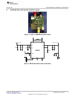
Evaluation Board Schematic and PCB Layout
8
Evaluation Board Schematic and PCB Layout
Figure 1. Picture of LM3269 Evaluation Board
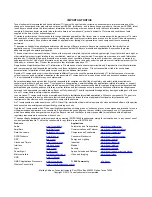
Figure 2. LM3269 Evaluation Board Schematic
3
SNVU162 – FEBRUARY 2013
LM3269 Evaluation Board
Submit Documentation Feedback
Copyright © 2013, Texas Instruments Incorporated


