


Other Functions
5.4
Device
Selects the TX channel (0 or 1) devices that the GUI is communicating with on the GC5325 EVM. This
includes the GC5325, DAC5682Z, and attenuator.
5.5
Port
Do not use.
5.6
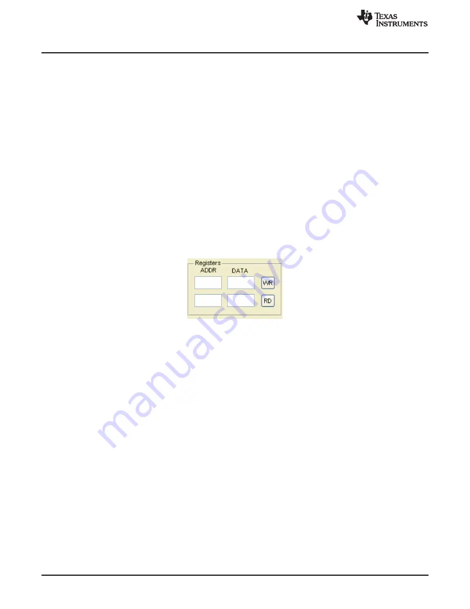
GC5325 Registers
The GC5325 Registers window (see
) allows the user to manually write and read the GC5325
internal registers. To write to a specific register, input the address and data in hexadecimal representation
in the top boxes in the Registers box, and then click the WR button.
To manually read the GC5325 registers, input the address in hexadecimal representation in the bottom-left
box in the Registers box, and click the RD button. The read value is then displayed in the Data box.
Another option is to uses scripts. Clicking on the "Script" button brings up a file browser to let you open a
script file to run. The first character of the script file must be e or E, followed by white space, then the
string to evaluate. No quote marks are needed. You can do multiple commands, but only on one line. The
following example will open two figures and displays the number "1" followed by "2".
The content of myScriptExample.txt:
e for index = 1:2 figure(index); disp(num2str(index)); end
Figure 22. GC5325 Register Window
5.7
Signal Setup.
Input rate (MSPS) - This is the data rate of the baseband signal. The GUI will resample the data to align
with the VCXO that is currently used on the EVM.
EVM Clock - This section specifies which clock source to use. The on-board VCXO is 737.28 MSPS. If
this source is bypassed to use an external source, the user needs to select the CLK option and enter the
frequency to be used.
Signal Display - This is used to display various plots of the input signal.
CFR Setup - The Auto option generates a filter based on the composite input signal. The Load option is
used to load in a predefined CFR filter.
This filter would be loaded during the process of loading the input test signal. To load a custom CFR filter,
select the Load option in the CFR setup section of the main GUI, as shown in
22
GC5325 System Evaluation Kit
SLWU063F
–
April 2009
–
Revised April 2011
Copyright
©
2009
–
2011, Texas Instruments Incorporated


