background image

Using the Software

www.ti.com

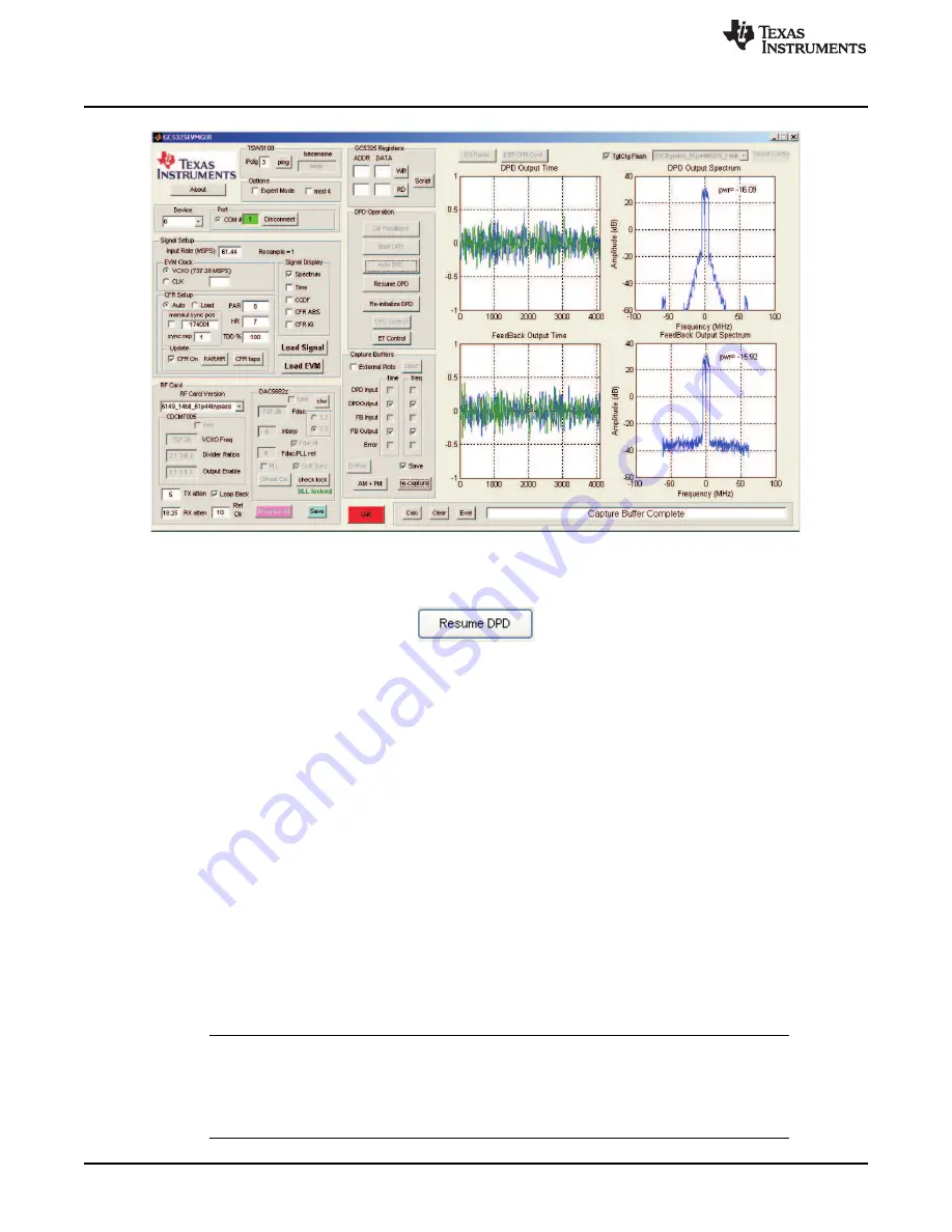
Figure 19. DPD Results From Internal PA for Channel 0

3. To resume adaption, click on Resume DPD.

The GUI then returns to the state where only Hold DPD and Re-initialize DPD buttons are active.

4. To restart DPD from the default loaded settings, click on the Re-initialize button. After clicking on

Re-initialize, the user can adjust the CFR PAR and Headroom, CFR taps, TX Atten, Loopback, etc. If
the TX atten setting is changed, a new Cal Feedback must be done.

4.2.2

Using External PAs

1. When operating with external PAs, the Loop Back mode must be disabled. When loop back is turned

off for Channel 0, LED D6 turns off and LED D8 now turns on, indicating that Channel 0 is now
transmitting across SMA connector J17 (TX0_OUT), and that the feedback path is now set up for
RX0_IN. For this case, the feedback signal must be connected to SMA connector J46 (RX0_IN).

2. When using an external PA for Channel 1, disable Loop Back. LED D5 turns off and LED D7 now turns

on, indicating that Channel 1 is now transmitting across SMA connector J18 (TX1_OUT), and that the
feedback path is now set up for RX1_IN. For this case, the feedback signal must be connected to SMA
connector J28 (RX1_IN).

3. When both channels are driving external PAs and running DPD, both LEDs D7 and D8 are blinking.

When a channel is using the feedback path, the LED is on. Both lights blinking indicate that both
channels are sharing the single feedback path.

4. After completing testing of the GC5325SEK, always shut down the GUI before removing power from

the system. To close the GUI, click on the Quit button located at the bottom of the GUI, or click on the
X in the upper right corner of the GUI window.

NOTE:

If at any time during operation of the GC5325SEK GUI, the following error appears (as

shown in

Figure 20

), just wait a second or two, then retry the last command that was

attempted. In most cases, the DSP recovers and executes the next command. If a problem
still exists, the DSP is probably locked, and the software must be closed, and reset the
hardware by either pressing the DSP reset switch or cycling the power.

20

GC5325 System Evaluation Kit

SLWU063F

April 2009

Revised April 2011

Submit Documentation Feedback

Copyright

©

2009

2011, Texas Instruments Incorporated

Summary of Contents for GC5325

Page 1: ...Sequence 6 3 Software Installation 7 3 1 MATLAB Control Libraries and Tools 7 3 2 TSW3100 Software and Drivers 7 3 3 DSP Weuffen USB to UHPI Software and Driver 7 4 Using the Software 8 4 1 Starting t...

Page 2: ...21 21 TXEQ Panel 21 22 GC5325 Register Window 22 23 CFR Setup Window 23 24 CFR Tap files directory 23 25 DPD CFR Configuration Window 24 26 DAC5682Z Offset Correction Window 26 27 DPD Control Window...

Page 3: ...optional onboard loopback to feedback path The RF section of the board also features a shared feedback path which consists of RF switches control shared feedback DSA and a mixer to convert to IF At th...

Page 4: ...connector J23 The GC5325EVM converts the 19 Vdc down to the required voltages needed by the board as well as generate the 4 5 5 Vdc for the TSW3100 Connect the provided power supply to connector J7 o...

Page 5: ...er must make sure the LO source frequency is set to match the configuration of the board To support the two operating frequency ranges the receive path contains two separate RF mixers along with a wid...

Page 6: ...2 OPEN CLOSED 147 45 MHz 672 MHz DIVIDE BY 2 OPEN OPEN 112 MHz 672 MHz DIVIDE BY 2 CLOSED OPEN 134 4 MHz 672 MHz DIVIDE BY 2 OPEN CLOSED 134 4 MHz 672 MHz DIVIDE BY 3 OPEN OPEN 74 6 MHz 672 MHz DIVID...

Page 7: ...00 The software driver installation procedure for this product can be found in the TSW3100EVM User s Guide and must be installed now if it has not already been installed The TSW3100EVM User s Guide an...

Page 8: ...t the installation After the installation is complete click on Finish If the default location was used the software is now loaded under the directory called C GC5325GUI Go to this folder and double cl...

Page 9: ...2 Select UHPI BOOT located in the upper right side of the GUI 3 Select UHPI in the left side of the GUI 4 Select DSP in the RF Port Options box located in the bottom right hand corner of the GUI The G...

Page 10: ...age Ratio PAR Headroom HR and TDD for the CFR block Referring to the following diagram Headroom is the clipping threshold relative to full scale for the CFR block and PAR is the RMS level of the input...

Page 11: ...ex MATLAB vector saved as a mat file Figure 8 or a two column text file Because the GC5325EVMGUI rescales the input signal to the appropriate RMS level the input signal can be floating point and need...

Page 12: ...er loading The first three are the Spectrum Figure 10 ABS time series Figure 11 and CCDF Figure 12 of the resampled signal Figure 10 Spectrum Figure 11 ABS Time Series 12 GC5325 System Evaluation Kit...

Page 13: ...ens The Autocfr_gui is a fast simple method to design the CFR cancellation filter based on the spectrum of the input signal The CFR filter has approximately the same spectral mask as the input signal...

Page 14: ...input signal If unchecked the entire input signal spectrum is used It is recommended to first get the basic CFR filter spectral shape as desired then uncheck Fast Design and regenerate This removes so...

Page 15: ...rd the three LEDs that indicate the status of the CDCM7005 see Figure 15 should now all be illuminated Figure 15 CDCM7005 Status LEDs 15 SLWU063F April 2009 Revised April 2011 GC5325 System Evaluation...

Page 16: ...are set properly 2 Make sure the USB cable is installed between the USB to UHPI board and the host PC 3 Make sure the DSP Weuffen drivers are installed properly 4 Make sure the USB to UHPI board is in...

Page 17: ...rd and the host with power applied to the board If these LEDs are not on try cycling the TSW3100 power and rebooting the host computer Other things to try are the following 1 Disconnect the USB Ethern...

Page 18: ...disabled the channel is transmitting through this SMA and the LED is off On power up both channels come up in loop back mode to prevent from possibly overdriving external PAs For Channel 1 LED D5 is i...

Page 19: ...ce DPD starts the system continues to adapt until the Hold DPD command is issued All buttons except for Hold DPD and Re initialize DPD are disabled To do any action such as capturing buffers reloading...

Page 20: ...ing across SMA connector J18 TX1_OUT and that the feedback path is now set up for RX1_IN For this case the feedback signal must be connected to SMA connector J28 RX1_IN 3 When both channels are drivin...

Page 21: ...to open a new window Then click on the TXEQ Plot button to generate the plot To invert the feedback signal spectrum click on the invert_eq_fb_flag box After doing this the user must re initialize DPD...

Page 22: ...ands but only on one line The following example will open two figures and displays the number 1 followed by 2 The content of myScriptExample txt e for index 1 2 figure index disp num2str index end Fig...

Page 23: ...such files under the C GC5325GUI cfr_tap_files directory Choose a custom taps file to be loaded for the CFR coefficients When the Import Wizard opens click on Next then Finish PAR This box specifies t...

Page 24: ...the DSP will use to calculate the CFR filter coefficients based on carrier prototype filters To enable the DSP CFR CONF button the user must first click on the Expert Mode option This is different fro...

Page 25: ...he maximum attenuation RX atten This box is used to set the attenuation value of the RX attenuator The range is from 0 to 31 75 using increments of 0 25 with 0 being minimum attenuation and 31 75 the...

Page 26: ...for each although typically only a value of 9 or less is needed Lowering the value will speed up the adaption time of the algorithm In most cases the Model and Z 0 values should be the same and the Z...

Page 27: ...rs AM PM This button makes either a PA AM AM amplitude vs amplitude plot as shown in Figure 28 or a AM PM plot amplitude vs phase The blue curve was taken before DPD The green and red ones were taken...

Page 28: ...SP and SPI bus is currently processing Commands can also be issued by entering the appropriate text in this widow and clicking on the Eval button This feature is not recommend to be used The Clear but...

Page 29: ...OS output clock See TSW3100 User s All set to Open Guide for more information SW1 Board main power switch ON SW5 External 1 8 Vdc and 3 3 VDC output supply Not used with the GC5325SEK OFF S9 FPGA Conf...

Page 30: ...emove for 1 2 external VCXO operation SJP14 GC5325 clock buffer control 2 3 SJP15 GC5325 clock buffer control 2 3 JP1 10MHz REF POWER Set to pins 2 3 when using external reference source 1 2 JP2 10MHz...

Page 31: ...de master clock to the TSW3100 J18 CH1 TX Output J36 CH1 TX output test connector after amplifier and attenuator J39 CH1 loopback test connector J28 TX1 feedback input connector RX1_IN J21 FB RF test...

Page 32: ...e VCXO may be converted to external if desired by moving shunts on two jumpers to power off the onboard VCXO Remove shunt on SJP16 and SJP17 Add shunt on SJP16 pins 1 2 and shunt SJP17 pins 2 3 An 8 d...

Page 33: ...t This notice contains important safety information about temperatures and voltages For additional information on TI s environmental and or safety programs please contact the TI application engineer o...

Page 34: ...orized for use in safety critical applications such as life support where a failure of the TI product would reasonably be expected to cause severe personal injury or death unless officers of the parti...

Page 35: ...Mouser Electronics Authorized Distributor Click to View Pricing Inventory Delivery Lifecycle Information Texas Instruments GC5325SEK...

Reviews: