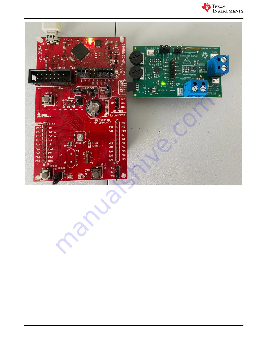
Figure 2-1. MSP-EXP430FR5969 LaunchPad connected to EVM
Power Connectors
www.ti.com
4
DRV821xEVM and DRV8220EVM User's Guide
SLOU540A – NOVEMBER 2020 – REVISED DECEMBER 2020
Submit Document Feedback
Copyright © 2020 Texas Instruments Incorporated
Page 1: ...ous current of both channels be limited to 0 9 A RMS when operating for extended periods of time at an ambient temperature of 25 C Table of Contents 1 Introduction 3 2 Power Connectors 3 3 Test Points...
Page 2: ...CB Top 3 D View Figure 1 2 PCB Assembly View PCB Top Assembly View www ti com 2 DRV821xEVM and DRV8220EVM User s Guide SLOU540A NOVEMBER 2020 REVISED DECEMBER 2020 Submit Document Feedback Copyright 2...
Page 3: ...FR5969 Note that a four pin angled male header is required and must be soldered to J21 of this Launchpad from V pin to GND pin We recommend a pin header with pin dimensions similar to 850 10 050 20 00...
Page 4: ...0FR5969 LaunchPad connected to EVM Power Connectors www ti com 4 DRV821xEVM and DRV8220EVM User s Guide SLOU540A NOVEMBER 2020 REVISED DECEMBER 2020 Submit Document Feedback Copyright 2020 Texas Instr...
Page 5: ...SE output from the current sense amplifier U4 R2 R3 R4 R16 and R19 can be removed to connect external MCU to J4 J2 Header use to set the state of the MODE nSLEEP signal MODE nSLEEP can be set to eithe...
Page 6: ...DRV821xDSG are EN IN1 and PH IN2 The functions of these inputs are IN1 and IN2 when the MODE is GND PWM mode or Hi Z independent half bridge mode When MODE is connected to 3 3 V PH EN control mode the...
Page 7: ...4 2 MODE nSLEEP jumper configuration for PH EN Table 4 1 PH EN Control Mode EN PH OUT1 OUT2 Description LOW turn IN1 PWM Pot completely counter clockwise X L L Brake Low Side Slow Decay PWM set IN1 PW...
Page 8: ...IN1 PWM pot in any position LOW turn PH IN2 PWM pot completely counter clockwise H L Forward OUT1 OUT2 HIGH turn EN IN1 PWM pot completely clockwise HIGH turn PH IN2 PWM pot completely clockwise L L B...
Page 9: ...is shown in Table 4 4 Figure 4 4 MODE nSLEEP does not require a jumper for independent half bridge mode Table 4 4 Independent Half Bridge Control Mode INx OUTx Description LOW turn INx PWM pot comple...
Page 10: ...not populated on the EVM The user needs to populate C11 with a desired value The current sense amplifier and the surrounding components R17 R18 and C6 are not populated on the EVM The user needs to p...
Page 11: ...s populated and no power is being supplied to the EVM 2 Short EN IN1 and PH IN2 pins on J4 with a jumper See Figure 6 1 3 Short OUT1 and OUT2 at connector J3 with an unexposed small wire or short the...
Page 12: ...nd low side driver for two loads DRV821xDSG VM 1 OUT1 2 OUT2 3 GND 4 VCC 8 MODE 7 IN1 6 IN2 5 Thermal Pad BDC 0 1 F CBulk VM 0 1 F Controller PWM VCC O X RLimit Figure 6 3 Half bridge mode used as a h...
Page 13: ...a a jumper to enable the device 5 If the DRV821xPDSG is populated connect the MODE nSLEEP header to 3 3V to set nSLEEP logic high and enable the device The MODE pin becomes the nSLEEP pin for the PDSG...
Page 14: ...ate the appropriate resistors Table 7 2 show the unique device ID for each supported device and the resistor combination to populate Table 7 1 Procedure For Soldering New Device and Passives to EVM Ne...
Page 15: ...0DSG ID1 1 ID2 1 ID3 0 R5 R7 R14 DRV8220DRL ID1 1 ID2 1 ID3 1 R5 R7 R8 8 Revision History NOTE Page numbers for previous revisions may differ from page numbers in the current version Changes from Revi...
Page 16: ...e resources are subject to change without notice TI grants you permission to use these resources only for development of an application that uses the TI products described in the resource Other reprod...