Figure 9-14. Board Dimensions
www.ti.com
Layout
SLVUC11 – APRIL 2021
Submit Document Feedback
DP83561EVM User’s Guide
45
Copyright © 2021 Texas Instruments Incorporated
Page 1: ...aterials see the associated sections and support documents DP83561EVM consists of a main PCB and two breakout boards DP83561 SP Ethernet board MAC interface breakout board and MAC interface back to ba...
Page 2: ...6 9 6 Signal Layer 2 37 9 7 Ground Layer 2 38 9 8 Bottom Layer 39 9 9 Bottom Layer Mask 40 9 10 Bottom Overlay 41 9 11 Board Assembly 42 10 Bill of Materials 46 11 REACH Compliance 54 12 Revision Hist...
Page 3: ...yer 39 Figure 9 9 Bottom Layer Mask 40 Figure 9 10 Bottom Overlay 41 Figure 9 11 Top Assembly 42 Figure 9 12 Bottom Assembly 43 Figure 9 13 Drill Drawing 44 Figure 9 14 Board Dimensions 45 List of Tab...
Page 4: ...I Reduced Gigabit Media Independent Interface MII Media Independent Interface SFD Start of Frame Detection VDDA Analog Core Supply Rail VDDIO Digital Supply Rail PD Pulldown PU Pullup MC Microcontroll...
Page 5: ...er supply or through a microUSB cable Note The DP83561EVM uses DP83561 SP Engineering Module EM parts EM parts do not ensure radiation performance They are suitable for prototyping but not suitable fo...
Page 6: ...Figure 2 1 DP83561EVM Top Side Introduction www ti com 6 DP83561EVM User s Guide SLVUC11 APRIL 2021 Submit Document Feedback Copyright 2021 Texas Instruments Incorporated...
Page 7: ...Figure 2 2 DP83561EVM Bottom Side www ti com Introduction SLVUC11 APRIL 2021 Submit Document Feedback DP83561EVM User s Guide 7 Copyright 2021 Texas Instruments Incorporated...
Page 8: ...2 2 Block Diagram Figure 2 3 DP83561EVM Block Diagram Introduction www ti com 8 DP83561EVM User s Guide SLVUC11 APRIL 2021 Submit Document Feedback Copyright 2021 Texas Instruments Incorporated...
Page 9: ...ns 2 and 3 Ensure shunt removed at J23 to disconnect VDDA1P8 LDO not needed in dual supply mode Place shunt at J20 to connect VDDA2P5 LDO Place shunt at P2 in the 3 3 V position to connect VDDIO LDO E...
Page 10: ...Figure 2 6 DP83561EVM Mirror Mode Strap Introduction www ti com 10 DP83561EVM User s Guide SLVUC11 APRIL 2021 Submit Document Feedback Copyright 2021 Texas Instruments Incorporated...
Page 11: ...e pulled high which can be done by placing a shunt on J35 If 1 8 V is used asthe VDDIO level both the VDDIOSEL_1 and VDDIOSEL_0 straps must be pulled high by placing shunts on J35 and J36 For a VDDIO...
Page 12: ...SB Power Supply Option DP838561EVM block powered by USB Place shunt at J23 to connect VDDA1P8 LDO triple supply mode only Place shunt at J20 to connect VDDA2P5 LDO Place shunt at P2 in desired VDDIO l...
Page 13: ...RGOOD 59 POWERGOOD 0 OPEN N A 1 CLOSED Table 3 4 DP83561 SP LED Bootstrap Selection and Jumper Designation PIN NAME PIN NUMBER STRAP NAME STRAP MODE JUMPER PLACEMENT JUMPER DESIGNATION LED_0 63 ANED_D...
Page 14: ...MII MAC Note RGMII back to back connector is reversible RGMII back to back breakout connector can be conneted to a DP83561EVM on either J19 or J22 DP83561EVM B DP83561EVM A RGMII back to back Breakout...
Page 15: ...T link established By default LED2 indicates RX TX activity 3 6 Serial Management Interface The DP83561EVM supports SMI MDIO MDC through J43 and includes an on board MSP for USB 2 MDIO control Notes D...
Page 16: ...sheet RGMII BER Testing External Loopback Configuration The DP83561EVM support RGMII BER testing through an external loopback configuration using the MAC Interface Breakout Board The MAC Interface Br...
Page 17: ...lease refer to the device data sheet MII MAC DP83561EVM MAC Interface Breakout Link Partner Cable Figure 4 2 DP83561EVM BER Testing MII Connection Diagram www ti com BER Testing SLVUC11 APRIL 2021 Sub...
Page 18: ...an RJ45 connector on J16 Please refer to the device datasheet for details on setting the different Ethernet Compliance Test Modes Figure 5 1 DP83561EVM Compliance Test Fixture Connection Compliance Te...
Page 19: ...J8 ECC Configuration Register Monitor If any change in the configuration registers are detected or corrected by the ECC an interrupt on the INT_CHECKSUM_N signal will be raised for indication to the h...
Page 20: ...nal 2 2k pull up resistor The resistors R42 R43 and R44 respectively may be replaced with a 2 2k resistor and connected to VDDIO VDDIO can be accessed via pins 2 4 and 6 of header P2 SEFI Support Moni...
Page 21: ...l ti com msp430 msp430_public_sw mcu msp430 MSP430_FET_Drivers latest index_FDS html 7 2 USB 2 MDIO Software Download the software from http www ti com tool usb 2 mdiohttps www ti com tool usb 2 mdio...
Page 22: ...8 Schematics Schematics www ti com 22 DP83561EVM User s Guide SLVUC11 APRIL 2021 Submit Document Feedback Copyright 2021 Texas Instruments Incorporated...
Page 23: ...VDDA1P8 VDDA2P5 VDDIO GND 5V USB_VBUS Wide Vin Supply 5V 36V VDD1P8 Sup ply VDD2P5 Sup ply VDD3P3 Sup ply VDD1P0 Sup ply Supply LED Indication Power Sup ply Selection 0 R21 5V 1 87k R28 4 99k R30 22uF...
Page 24: ...C 54 MDIO 53 RBIAS 15 RESET POWERGOOD 59 SMI_DISABLE 50 SUPPLYMODESEL 23 TX_EN TX_CTRL 48 XI 26 XO 25 RX_CLK 42 RX_DV RX_CTRL 49 RX_ER 43 RX_D0 44 RX_D1 45 RX_D2 46 RX_D3 47 INT_ECC 56 INT PWDN 60 INT...
Page 25: ...R164 2 49k R165 2 49k R167 2 49k R169 2 49k R172 VDDIOSEL_1 VDDIOSEL_0 SUPPLYMODESEL AUTO_RECOVER SMI_DISABLE 2 49k R173 CRS Green 1 2 LD4 CMP 0002917 2 Green 1 2 LD3 CMP 0002917 2 Green 1 2 LD6 CMP 0...
Page 26: ...MP3 MP4 MP4 J4 ERM8 030 01 L D EM2 TR RX_ER COL 1 2 J5 TSW 102 07 G S GND GND 0 R13 RX_ER_CS RX_ER 0 R33 0 R32 COL CRS COL_CS CRS_CS GND MAC Interface RGMII MII MDI Copper Interf ace 2 1 3 22 24 23 4...
Page 27: ...47k R198 27 R196 27 R199 22 R181 22 R182 22 R184 22 R185 22 R192 22 R193 15 0k R186 15 0k R187 15 0k R194 15 0k R195 15 0k R188 15 0k R189 15 0k R190 15 0k R191 10k R179 1 00M R200 1 50k R178 1 40k R...
Page 28: ...R68 P1 1 GND GND TARGET_D_N 1 00M R74 GND TARGET_PUR 1 40k R73 TARGET_D_P TEST SBWTCK RST SBWTDIO 470 R69 470 R70 USB_VBUS MCU_VCC MCU_VCC 0 1 F C22 0 1 F C24 0 1 F C23 0 22uF C17 0 22uF C20 470nF C1...
Page 29: ...20 P1 3 TA0 2 21 P1 4 TA0 3 22 P1 5 TA0 4 23 P1 6 TA1CLK CBOUT 24 P1 7 TA1 0 25 P2 0 TA1 1 26 P2 1 TA1 2 27 P2 2 TA2CLK SMCLK 28 P2 3 TA2 0 29 P2 4 TA2 1 30 P2 5 TA2 2 31 P2 6 RTCCLK DMAE0 32 P2 7 UCB...
Page 30: ...34 35 36 37 38 39 40 41 42 43 44 45 46 47 48 49 50 51 52 53 54 55 56 57 58 59 60 MP1 MP1 MP2 MP2 MP3 MP3 MP4 MP4 J22 ERF8 030 01 L D EM2 TR MDC_2 MDIO_2 RX_ER_2 COL_2 CRS_2 RESETN_2 RX_CTRL_2 TX_CTRL...
Page 31: ...CMP 0077181 1 FID15 CMP 0077181 1 FID16 CMP 0077181 1 FID17 CMP 0077181 1 FID18 CMP 0077181 1 SH J1 M7582 05 SH J2 M7582 05 SH J3 M7582 05 SH J4 M7582 05 SH J5 M7582 05 SH J6 M7582 05 SH J7 M7582 05 S...
Page 32: ...9 Layout 9 1 Top Overlay Figure 9 1 Top Overlay Layout www ti com 32 DP83561EVM User s Guide SLVUC11 APRIL 2021 Submit Document Feedback Copyright 2021 Texas Instruments Incorporated...
Page 33: ...9 2 Top Layer Mask Figure 9 2 Top Layer Mask www ti com Layout SLVUC11 APRIL 2021 Submit Document Feedback DP83561EVM User s Guide 33 Copyright 2021 Texas Instruments Incorporated...
Page 34: ...9 3 Top Layer Figure 9 3 Top Layer Layout www ti com 34 DP83561EVM User s Guide SLVUC11 APRIL 2021 Submit Document Feedback Copyright 2021 Texas Instruments Incorporated...
Page 35: ...9 4 Ground Layer 1 Figure 9 4 Ground Layer 1 www ti com Layout SLVUC11 APRIL 2021 Submit Document Feedback DP83561EVM User s Guide 35 Copyright 2021 Texas Instruments Incorporated...
Page 36: ...9 5 Signal Layer 1 Figure 9 5 Signal Layer 1 Layout www ti com 36 DP83561EVM User s Guide SLVUC11 APRIL 2021 Submit Document Feedback Copyright 2021 Texas Instruments Incorporated...
Page 37: ...9 6 Signal Layer 2 Figure 9 6 Signal Layer 2 www ti com Layout SLVUC11 APRIL 2021 Submit Document Feedback DP83561EVM User s Guide 37 Copyright 2021 Texas Instruments Incorporated...
Page 38: ...9 7 Ground Layer 2 Figure 9 7 Ground Layer 2 Layout www ti com 38 DP83561EVM User s Guide SLVUC11 APRIL 2021 Submit Document Feedback Copyright 2021 Texas Instruments Incorporated...
Page 39: ...9 8 Bottom Layer Figure 9 8 Bottom Layer www ti com Layout SLVUC11 APRIL 2021 Submit Document Feedback DP83561EVM User s Guide 39 Copyright 2021 Texas Instruments Incorporated...
Page 40: ...9 9 Bottom Layer Mask Figure 9 9 Bottom Layer Mask Layout www ti com 40 DP83561EVM User s Guide SLVUC11 APRIL 2021 Submit Document Feedback Copyright 2021 Texas Instruments Incorporated...
Page 41: ...9 10 Bottom Overlay Figure 9 10 Bottom Overlay www ti com Layout SLVUC11 APRIL 2021 Submit Document Feedback DP83561EVM User s Guide 41 Copyright 2021 Texas Instruments Incorporated...
Page 42: ...9 11 Board Assembly Figure 9 11 Top Assembly Layout www ti com 42 DP83561EVM User s Guide SLVUC11 APRIL 2021 Submit Document Feedback Copyright 2021 Texas Instruments Incorporated...
Page 43: ...Figure 9 12 Bottom Assembly www ti com Layout SLVUC11 APRIL 2021 Submit Document Feedback DP83561EVM User s Guide 43 Copyright 2021 Texas Instruments Incorporated...
Page 44: ...Figure 9 13 Drill Drawing Layout www ti com 44 DP83561EVM User s Guide SLVUC11 APRIL 2021 Submit Document Feedback Copyright 2021 Texas Instruments Incorporated...
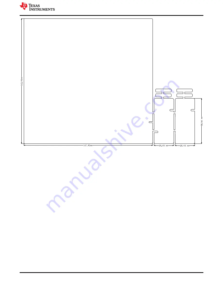
Page 45: ...Figure 9 14 Board Dimensions www ti com Layout SLVUC11 APRIL 2021 Submit Document Feedback DP83561EVM User s Guide 45 Copyright 2021 Texas Instruments Incorporated...
Page 46: ...20 2 0 22uF CAP CERM 0 22 uF 16 V 80 20 Y5V 0603 0603 C0603C224Z4VACTU Kemet C18 1 0 47uF CAP CERM 0 47 uF 16 V 10 X7R AEC Q200 Grade 1 0603 0603 GCM188R71C474KA55D MuRata C19 1 4 7uF CAP CERM 4 7 uF...
Page 47: ...0 X7R AEC Q200 Grade 1 0603 0603 CGA3E3X7R1H224K080AB TDK C74 C75 C76 C77 C84 5 22uF CAP CERM 22 uF 16 V 20 X7R AEC Q200 Grade 1 1210 1210 CGA6P1X7R1C226M250AC TDK C82 1 0 01uF CAP CERM 0 01 F 50 V 5...
Page 48: ...N A N A H1 H2 H3 H4 H5 H6 H7 H8 8 Standoff Hex 0 5 L 4 40 Nylon Standoff 1902C Keystone J1 J19 J22 3 Receptacle 0 8mm 30x2 Gold Edge Mount Receptacle 0 8mm 30x2 Edge Mount ERF8 030 01 L D EM2 TR Samt...
Page 49: ...2 1 Header 100mil 3x2 Gold TH 3x2 Header TSW 103 07 G D Samtec Q1 Q2 Q3 Q4 4 60 V Transistor NPN 60 V 1 A AEC Q101 SOT 23 SOT 23 DNBT8105 7 Diodes Inc R1 R2 R79 R102 R103 R104 R105 R147 R149 R157 R161...
Page 50: ...1 00Meg RES 1 00 M 1 0 1 W 0402 0402 ERJ 2RKF1004X Panasonic R40 R41 2 200k RES 200 k 5 0 1 W AEC Q200 Grade 0 0603 0603 CRCW0603200KJNEA Vishay Dale R48 R51 R62 R63 R64 R65 R66 R67 8 2 20k RES 2 20...
Page 51: ...00 1 4 22k RES 4 22 k 1 0 1 W AEC Q200 Grade 0 0603 0603 CRCW06034K22FKEA Vishay Dale R106 1 10 0k RES 10 0 k 1 0 1 W 0603 0603 RC0603FR 0710KL Yageo R107 R114 R117 R123 4 75 0 RES 75 0 1 0 063 W AEC...
Page 52: ...Instruments U5 1 Hi Reliability High Immunity Radiation Resistant Gigabit Ethernet PHY CFP64 DP83561HBE EM Texas Instruments U6 1 3 8 V to 36 V 2 A Synchronous Step Down Voltage Regulator RNX0012B VQ...
Page 53: ...140 R142 R144 0 0 RES 0 5 0 1 W AEC Q200 Grade 0 0402 0402 ERJ 2GE0R00X Panasonic R84 0 0 RES 0 5 0 1 W 0603 0603 RC0603JR 070RL Yageo R152 R155 0 6 04k RES 6 04 k 1 0 063 W AEC Q200 Grade 0 0402 0402...
Page 54: ...urer Component Type Component Part Number SVHC Substance SVHC CAS when available Murata Resonant Ceramic Element CSTCR6M00G53Z R0 Lead Titanium Zirconium Oxide 16626 81 2 Murata Resonant Ceramic Eleme...
Page 55: ...ther than TI b the nonconformity resulted from User s design specifications or instructions for such EVMs or improper system design or c User has not paid on time Testing and other quality control tec...
Page 56: ...These limits are designed to provide reasonable protection against harmful interference in a residential installation This equipment generates uses and can radiate radio frequency energy and if not in...
Page 57: ...instructions set forth by Radio Law of Japan which includes but is not limited to the instructions below with respect to EVMs which for the avoidance of doubt are stated strictly for convenience and s...
Page 58: ...any interfaces electronic and or mechanical between the EVM and any human body are designed with suitable isolation and means to safely limit accessible leakage currents to minimize the risk of electr...
Page 59: ...R DAMAGES ARE CLAIMED THE EXISTENCE OF MORE THAN ONE CLAIM SHALL NOT ENLARGE OR EXTEND THIS LIMIT 9 Return Policy Except as otherwise provided TI does not offer any refunds returns or exchanges Furthe...
Page 60: ...are subject to change without notice TI grants you permission to use these resources only for development of an application that uses the TI products described in the resource Other reproduction and...