Texas Instruments AN-1622 LM49100 User Manual Download Page 8

Demonstration Board PCB Layout

www.ti.com

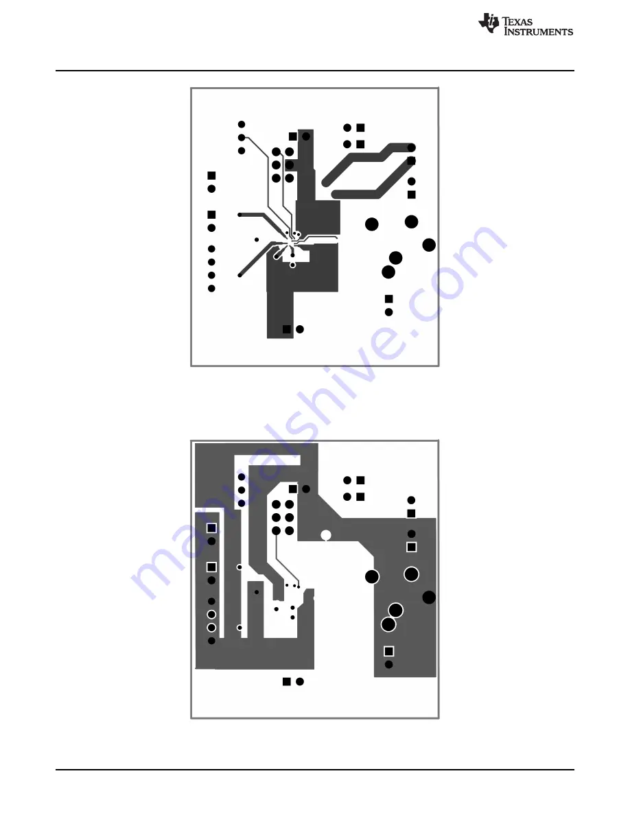
Figure 6. Upper Inner Layer

Figure 7. Lower Middle Layer

8

AN-1622 LM49100 Evaluation Board»

SNAA043A – October 2007 – Revised May 2013

Submit Documentation Feedback

Copyright © 2007–2013, Texas Instruments Incorporated

Summary of Contents for AN-1622 LM49100

Page 1: ...pin and HPR pin carries the output signals from the two amplifiers and each of the other pins connecting to ground making this configuration single ended connections 6 Differential mono amplifier outp...

Page 2: ...th a mono input signal The LM49100 features a 32 step digital volume control and ten distinct output modes The mixer volume control and device mode select are controlled through an I2 C compatible int...

Page 3: ...d is an I2 C signal generation board and software With this board and the software the user can easily control the LM49100 s shutdown function mute and stereo volume control Figure 2 shows the softwar...

Page 4: ...ation board VDDHP GND Headphone power supply for the headphone amplifier which creates split supplies for the positive voltage is converted by switch capacitor creating a negative voltage of equal mag...

Page 5: ...udes controls for the amplifier s volume control individual channel shutdown and the mute function The control program s on screen user interface is shown in Figure 2 The Default button is used to ret...

Page 6: ...r 0 1 F 0805 HPL 2 pin header 100 mil pitch 1x2 Header HPR 2 pin header 100 mil pitch 1x2 Header I2C 6 pin 6 pin header 100 mil pitch 2x3 Header Header Left Input 2 pin header 100 mil pitch 1x2 Header...

Page 7: ...ration Board PCB Layout Figure 4 Top Overlay Figure 5 Top Layer 7 SNAA043A October 2007 Revised May 2013 AN 1622 LM49100 Evaluation Board Submit Documentation Feedback Copyright 2007 2013 Texas Instru...

Page 8: ...yout www ti com Figure 6 Upper Inner Layer Figure 7 Lower Middle Layer 8 AN 1622 LM49100 Evaluation Board SNAA043A October 2007 Revised May 2013 Submit Documentation Feedback Copyright 2007 2013 Texas...

Page 9: ...ion Board PCB Layout Figure 8 Bottom Layer Figure 9 Bottom Overlay 9 SNAA043A October 2007 Revised May 2013 AN 1622 LM49100 Evaluation Board Submit Documentation Feedback Copyright 2007 2013 Texas Ins...

Page 10: ...5 respectively Typical THD N versus Output Power performance curves at VDD 3V 3 6V and 5V for 32 and 8 are shown in Figure 16 and Figure 17 respectively Figure 10 THD N vs Frequency Figure 11 THD N vs...

Page 11: ...ti com Typical Demonstration Board Audio Performance Figure 16 THD N vs Output Power Figure 17 THD N vs Output Power RL 32 f 1kHz RL 8 f 1kHz BW 22kHz HP Mode 4 BW 22kHz LS Mode 1 11 SNAA043A October...

Page 12: ...ed for extra headphone output attenuation Table 4 Output Mode Selection 1 Output Mode MC3 MC2 MC1 MC0 Handsfree Mono Output Right HP Output Left HP Output Number 0 0 0 0 0 SD SD SD 1 0 0 0 1 2 GM M SD...

Page 13: ...0 1 0 13 5 19 5 12 0 1 0 1 1 12 18 13 0 1 1 0 0 10 5 16 5 14 0 1 1 0 1 9 15 15 0 1 1 1 0 7 5 13 5 16 0 1 1 1 1 6 12 17 1 0 0 0 0 4 5 10 5 18 1 0 0 0 1 3 9 19 1 0 0 1 0 1 5 7 5 20 1 0 0 1 1 0 6 21 1 0...

Page 14: ...olling microcontroller and the slave is the LM49100 The I2 C address for the LM49100 is determined using the ADDR pin The LM49100 s two possible I2 C chip addresses are of the form 111110X10 binary wh...

Page 15: ...I2 C Bus Format Figure 20 I2 C Timing Diagram 15 5 I2 C Interface Power Supply Pin VDDI2 C The LM49100 s I2 C interface is powered up through theVDD I2 C pin The LM49100 s I2 C interface operates at...

Page 16: ...he single ended configuration its differential output doubles the voltage swing across the load Theoretically this produces four times the output power when compared to a single ended amplifier under...

Page 17: ...emperature If these measures are insufficient a heat sink can be added to reduce JA The heat sink can be created using additional copper area around the package with connections to the ground pin s su...

Page 18: ...ess shutdown function As discussed above choosing CIN no larger than necessary for the desired bandwidth helps minimize clicks and pops CB s value should be in the range of 4 to 5 times the value of C...

Page 19: ...y 18 Revision History Rev Date Description 1 0 10 1907 Initial release 19 SNAA043A October 2007 Revised May 2013 AN 1622 LM49100 Evaluation Board Submit Documentation Feedback Copyright 2007 2013 Texa...

Page 20: ...sponsible for compliance with all legal regulatory and safety related requirements concerning its products and any use of TI components in its applications notwithstanding any applications related inf...

Reviews: