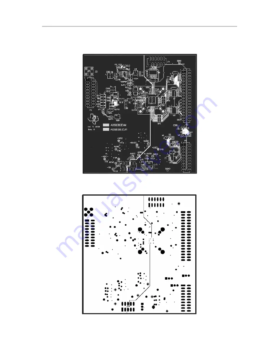
ADS8383EVM Layout
6-5
ADS8383EVM BOM, Layout, and Schematic
6.2
Figure 6−1. Top Layer—Layer 1
Figure 6−2. Ground Plane—Layer 2
Page 1: ...ADS8383EVM December 2003 Data Acquistion User s Guide SLAU119...
Page 2: ...itute a license from TI to use such products or services or a warranty or endorsement thereof Use of such information may require a license from a third party under the patents or other intellectual p...
Page 3: ...handling or use of the goods Please be aware that the products received may not be regulatory compliant or agency certified FCC UL CE etc Due to the open construction of the product it is the user s r...
Page 4: ...there is uncertainty as to the load specification please contact a TI field representative During normal operation some circuit components may have case temperatures greater than 60 C The EVM is desi...
Page 5: ...pter 3 Digital Interface Chapter 4 Power Supply Requirements Chapter 5 Using the EVM Chapter 6 ADS8383EVM BOM Layout and Schematic Related Documentation From Texas Instruments To obtain a copy of any...
Page 6: ...the limits of computing devices pursuant to subpart J of part 15 of FCC rules which are designed to provide reasonable protection against radio frequency interference Operation of this equipment in o...
Page 7: ...e 2 3 3 Digital Interface 3 1 4 Power Supply Requirements 4 1 5 Using the EVM 5 1 5 1 As a Reference Board 5 2 5 2 As a Prototype Board 5 2 5 3 As a Software Test Platform 5 2 6 ADS8383EVM BOM Layout...
Page 8: ...r Layer 4 6 5 2 1 Analog Input Connector 2 1 2 2 Sholder Short Jumper Setting 2 3 3 1 Pinout for Parallel Control Connector P2 3 1 3 2 Jumper Settings 3 2 3 3 Data Bus Connector P3 3 2 3 4 Pinout for...
Page 9: ...1 1 EVM Overview This chapter contains the features of the ADS8383EVM Topic Page 1 1 Features 1 1 Chapter 1...
Page 10: ...aluation board for the high speed ADS8383 18 bit single channel parallel interface SAR type analog to digital converters Onboard signal conditioning Onboard reference Input and output digital buffer O...
Page 11: ...of SMA connector J2 Table 2 1 Analog Input Connector Description Signal Name Connector Pin Signal Name Description Pin tied to Ground AGND P1 1 P1 2 Noninverting Input Channel Reserved N A P1 3 P1 4...
Page 12: ...at ADS8383EVM would meet the 100 kHz AC performance specifications listed in the data sheet The series resistor works in conjunction with the capacitor to filter the input signal but also isolates the...
Page 13: ...able 2 2 for jumper settings See Chapter 6 for the full schematic Table 2 2 Solder Short Jumper Setting Reference Description Jumper Setting Reference Designator Description 1 2 2 3 SJP1 Select REF304...
Page 14: ...2 4...
Page 15: ...ddress line from processor P2 11 A2 Address line from processor P2 13 P2 15 P2 17 P2 19 INTc Set jumper W3 to select BUSY or inverted signal to be applied to this pin Note All even numbered pins of P2...
Page 16: ...ta Bit 5 P3 13 D6 Buffered Data Bit 6 P3 15 D7 Buffered Data Bit 7 P3 17 D8 Buffered Data Bit 8 P3 19 D9 Buffered Data Bit 9 P3 21 D10 Buffered Data Bit 10 P3 23 D11 Buffered Data Bit 11 P3 25 D12 Buf...
Page 17: ...tion TP16 BVDD Apply 3 3 V or 5 0 V See ADC datasheet for full range TP20 AVCC Apply 5 0 V TP14 VA Apply 6 0 V Positive supply for amplifier TP18 VA Apply 6 0 V Negative supply for amplifier 2 Use the...
Page 18: ...4 2...
Page 19: ...8383EVM serves three functions 1 As a reference design 2 As a prototype board and 3 As software test platform Topic Page 5 1 As a Reference Board 5 2 5 2 As a Prototype Board 5 2 5 3 As a Software Tes...
Page 20: ...it shorts the minus supply pin of the amplifier to ground Positive supply voltage can be applied via test point TP14 or connector J1 pin 1 5 3 As a Software Test Platform As a software test platform...
Page 21: ...Layout and Schematic This chapter contains the ADS8383EVM bill of materials the layouts and the schematic Topic Page 6 1 ADS8383EVM Bill of Materials 6 2 6 2 ADS8383EVM Layouts 6 5 6 3 ADS8383EVM Sche...
Page 22: ...10W 1 0805 SMD 9 5 10k R16 R17 Panasonic ECG or ERJ 3EKF1002V Resistor 10 0 k 1 16W 1 9 5 10k R16 R17 R18 R19 Panasonic ECG or Alternate ERJ 3EKF1002V Resistor 10 0 k 1 16W 1 0603 SMD R18 R19 R20 Alt...
Page 23: ...ic ECG or Alternate ECJ 3YB0J226M Capacitor 22 F 6 3V ceramic X5R 1206 28 4 NI C13 C18 NOT INSTALLED NOT INSTALLED 28 4 NI C13 C18 C45 C60 NOT INSTALLED NOT INSTALLED 29 3 NI C30 C35 R5 NOT INSTALLED...
Page 24: ...SM 118 01 T D V P 0 025 SMT plug top side of PWB 48 2 10X2X 1 P1 P2 Samtec SSW 110 22 S D VS 0 025 SMT socket bottom side of PWB Samtec TSM 110 01 T D V P 0 025 SMT plug top side of PWB 49 2 SJP2 SJP3...
Page 25: ...ADS8383EVM Layout 6 5 ADS8383EVM BOM Layout and Schematic 6 2 ADS8383EVM Layout Figure 6 1 Top Layer Layer 1 Figure 6 2 Ground Plane Layer 2...
Page 26: ...ADS8383EVM Layout 6 6 Figure 6 3 Power Plane Layer 3 Figure 6 4 Bottom Layer Layer 4...
Page 27: ...ADS8383EVM Schematic 6 7 ADS8383EVM BOM Layout and Schematic 6 3 ADS8383EVM Schematic The schematic follows this page...
Page 28: ...Mouser Electronics Authorized Distributor Click to View Pricing Inventory Delivery Lifecycle Information Texas Instruments ADS8383EVM...