background image

User's Guide

SBAU233A – October 2014 – Revised November 2015

ADS8339EVM-PDK

ADS8339EVM-PDK

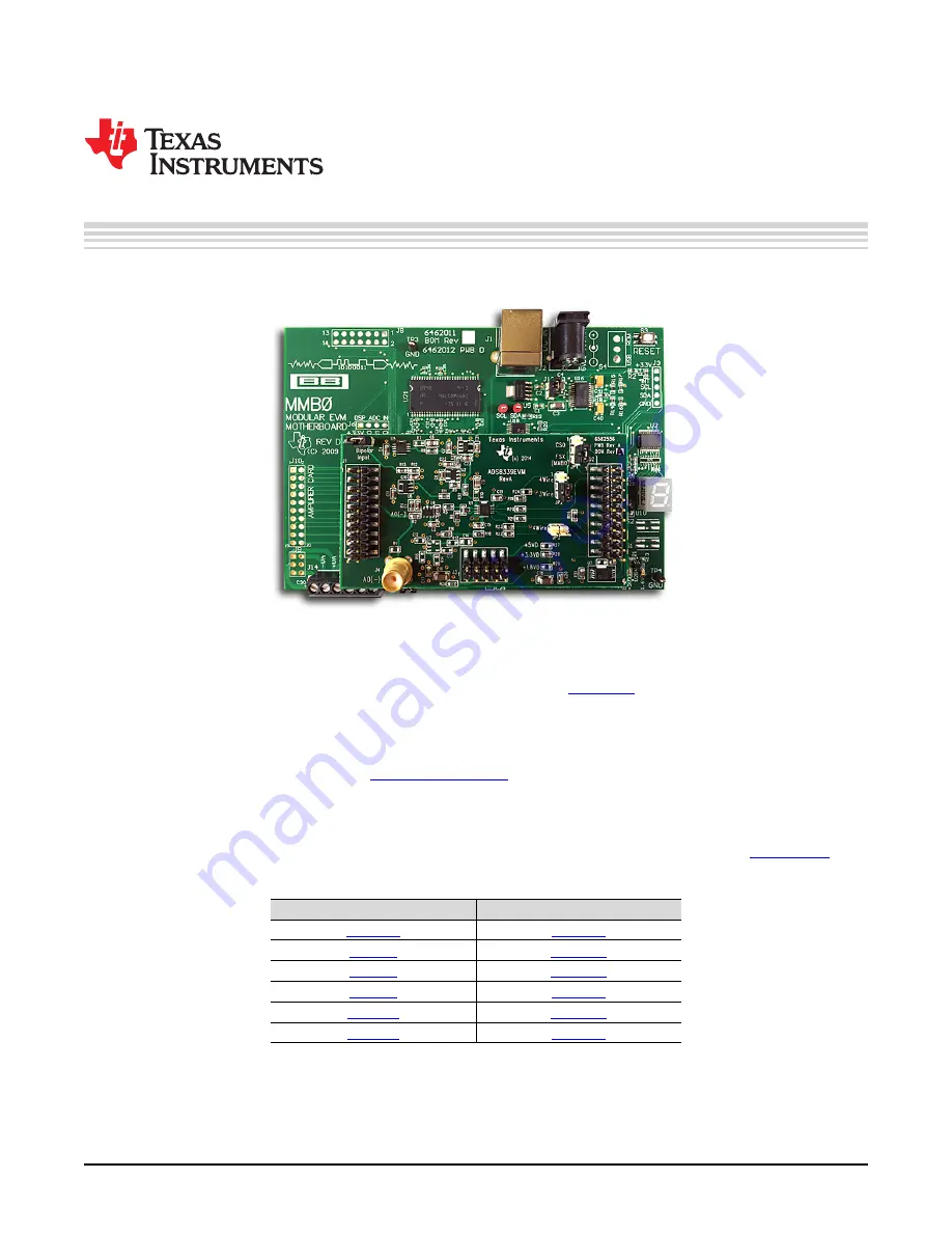
This user's guide describes the operation and use of the

ADS8339

evaluation module (EVM). The

ADS8339 is a 16-bit, pseudo-differential, unipolar, successive approximation register (SAR), analog-to-
digital converter (ADC) with a maximum throughput of 250-KSPS. The device is a very low-power ADC
with excellent noise and distortion performance for ac or dc signals. The performance demonstration kit
(PDK) eases EVM evaluation with additional hardware and software for computer connectivity through a
universal serial bus (USB). The

ADS8339EVM-PDK

includes the ADS8339EVM as a daughter card,

MMB0 motherboard, and an A-to-B USB cable. This user's guide covers circuit description, schematic
diagram, and bill of materials for the ADS8339EVM daughter card. Throughout this document, the
abbreviation EVM and the term evaluation module are synonymous with the ADS8339EVM-PDK.

The following related documents are available through the Texas Instruments web site at

www.ti.com

.

Related Documentation

Device

Literature Number

ADS8339

SBAS677

OPA333

SBOS351

OPA376

SBOS406

OPA836

SLOS712

REF5045

SBOS410

THS4281

SLOS432

ADCPro is a trademark of Texas Instruments.
Windows is a registered trademark of Microsoft Corporation.
SPI is a trademark of Motorola, Inc.
Samtec is a trademark of Samtec, Inc.
All other trademarks are the property of their respective owners.

1

SBAU233A – October 2014 – Revised November 2015

ADS8339EVM-PDK

Submit Documentation Feedback

Copyright © 2014–2015, Texas Instruments Incorporated

Summary of Contents for 296-38528-ND

Page 1: ... and an A to B USB cable This user s guide covers circuit description schematic diagram and bill of materials for the ADS8339EVM daughter card Throughout this document the abbreviation EVM and the term evaluation module are synonymous with the ADS8339EVM PDK The following related documents are available through the Texas Instruments web site at www ti com Related Documentation Device Literature Nu...

Page 2: ... Configuration 8 6 MMB0 Driver Installer 9 7 Plug In Installer 10 8 MMB0 Motherboard Jumper Configuration 11 9 ADS8339EVM Jumper Configuration 11 10 Loading EVM Plug In 12 11 ADS8339EVM Plug In Device Configuration Tab 13 12 ADCPro Test Plug ins 14 13 ADS8339EVM PCB Top Layer 16 14 ADS8339EVM PCB Ground Layer 16 15 ADS8339EVM PCB Power Layer 17 16 ADS8339EVM PCB Bottom Layer 17 17 Schematic 18 Lis...

Page 3: ... see SBAU128 ADCPro Analog to Digital Converter Evaluation Software User s Guide available for download from www ti com 1 1 ADS8339EVM Daughterboard Features Includes support circuitry as a design example to match ADC performance 3 3 V slave serial peripheral interface SPI Serial interface header for easy connection to TI DSP based communication systems Compatible with the TI Modular EVM system De...

Page 4: ...onnector Number Signal Description Samtec 10 2 J1 10 A0 CH0 inverted EVM input SMA J4 A0 CH0 inverted EVM input 2 1 Bipolar Input Signal Configuration With JP4 closed the OPA836 positive input is biased with 1 125 V created by diving the 4 5 V onboard reference by four This bias becomes a 2 25 V offset at the output of the OPA836 that allows input signals with a 0 V common mode voltage To keep the...

Page 5: ...is filtered by an RC filter with a 160 Hz cutoff frequency to minimize noise contribution The EVM is buffered by the THS4281 which drives the 10 μF capacitor required at the ADC reference input The OPA333 with additional feedback is optional but does complement the THS4281 and minimizes offset and drift Figure 3 THS4281 Reference Driver with Complementary OPA333 for Drift and Offset Correction 5 S...

Page 6: ...BUSY bit Direct connection to the convert start pin if JP3 is J2 17 CONVST installed J2 4 J2 10 and J2 18 GND Grounded pins I2 C bus used only to program the U4 EEPROM on J2 16 J2 20 I2 C bus the EVM board J2 2 J2 5 6 J2 8 9 J2 11 12 J2 14 and Unused Unused J2 19 3 1 Serial Interface SPI The ADS8339 ADC uses SPI serial communication to send conversion results to the MMB0 motherboard and subsequent...

Page 7: ...og Power Options The ADS8339EVM board functions with a 5 V supply provided at J3 3 by the MMB0 motherboard powering the onboard reference op amps and the analog supply of the ADS8339 4 2 Digital Power Options The ADS8339EVM connects the digital power supply of the ADS8339 to 3 3VD J3 10 to match the 3 3 V logic level of the MMB0 motherboard 4 3 Analog and Digital Grounds The EVM only has one groun...

Page 8: ...nd after the conversion time the falling edge of the chip select signal brings the digital output out of tri state mode Figure 4 shows the serial configuration for this mode Figure 4 Serial 3 Wire Configuration 5 2 SPI 4 Wire Mode JP2 1 2 and JP3 CLOSED The chip select signal is used to bring the ADS8339 digital output out of tri state However conversion is initialized from J3 17 as an independent...

Page 9: ... PDK hardware Step 5 Power up the ADS8339EVM PDK Each task is described in the subsequent sections of this document 6 1 Install ADCPro Software ADCPro is the primary program used to evaluate the ADS8339 ADCPro is available at www ti com tool adcpro Refer to SBAU128 ADCPro User s Guide for detailed installation instructions 6 2 Install MMB0 Motherboard Drivers NOTE The user must have administrator ...

Page 10: ...ction look for a link with a file named ads8339evm adcproplugin version exe where version refers to the installation file version number and increments with software version releases Download and double click the file and then follow the instructions Figure 7 shows the initial and completed installer screen shots Figure 7 Plug In Installer 10 ADS8339EVM PDK SBAU233A October 2014 Revised November 2...

Page 11: ...ulate the input down to 5 V 3 3 V and 1 8 V J13B must be closed This setting connects the 5 V analog power supply with the 5 V digital power supply J13A must be opened This setting allows the 5 V analog power supply to be regulated on board Figure 8 MMB0 Motherboard Jumper Configuration Step 3 Set JP1 2 3 JP2 2 3 JP3 open and JP4 closed on the ADS8339EVM as shown in Figure 9 Figure 9 ADS8339EVM Ju...

Page 12: ...re data 7 1 About MMB0 The MMB0 is a modular EVM system motherboard The MMB0 provides the USB interface between the PC and the ADS8339EVM The MMB0 is designed around the TMS320VC5509 a DSP with an onboard USB interface from Texas Instruments The MMB0 also has 16 MB of SDRAM installed The MMB0 is not sold as a DSP development board and is not available separately TI cannot offer support for the MMB...

Page 13: ...om 3 960 kSPS to 21 052 kSPS 2 SCLK By default SCLK is at 25 MHz SCLK sets the clock frequency used by the SPI interface to capture data Note that reducing SCLK frequency also reduces the maximum data rate 3 Reference 4 5 V is the default reference value and matches the onboard reference of the EVM To read accurate voltages set the value of this control to be the exact value of the reference 4 Dev...

Page 14: ... regarding how to set up and use the various test plug ins refer to SBAU128 ADCPro User s Guide 7 5 Acquire Data When the ADS8339EVM is configured for the desired test scenario press the Acquire button to start the data collection process The software collects the number of data points located in the test plug in Block Size field 512 by default see SBAU128 During data acquisition the ADS8339EVM pl...

Page 15: ... 22 F D VS K 13 1 J4 CONN SMA JACK STRAIGHT PCB Amphenol 132134 14 2 JP1 JP2 Header Strip 3 pin 100 Gold 1x3 Samtec TSW 103 07 L S 15 2 JP3 JP4 Header Strip 2 pin 100 Gold 1x2 Samtec TSW 102 07 L S 16 7 R1 R14 R15 R17 Do Not Install DNI R27 R29 R30 17 2 1k R2 R3 Resistor Metal Film Chip 0 1 1 10W 0603 Panasonic ERA 3AEB102V 18 1 100 R4 Resistor Thick Film Chip 1 1 10W 0603 Panasonic ERJ 3EKF1000V ...

Page 16: ...not to scale These figures are intended to show how the board is laid out they are not intended to be used for manufacturing ADS8339EVM PCBs Figure 13 ADS8339EVM PCB Top Layer Figure 14 ADS8339EVM PCB Ground Layer 16 ADS8339EVM PDK SBAU233A October 2014 Revised November 2015 Submit Documentation Feedback Copyright 2014 2015 Texas Instruments Incorporated ...

Page 17: ...ut and Schematic Figure 15 ADS8339EVM PCB Power Layer Figure 16 ADS8339EVM PCB Bottom Layer 17 SBAU233A October 2014 Revised November 2015 ADS8339EVM PDK Submit Documentation Feedback Copyright 2014 2015 Texas Instruments Incorporated ...

Page 18: ...rials Layout and Schematic www ti com 8 3 Schematic Figure 17 Schematic 18 ADS8339EVM PDK SBAU233A October 2014 Revised November 2015 Submit Documentation Feedback Copyright 2014 2015 Texas Instruments Incorporated ...

Page 19: ...e ADS8339EVM PDK in first paragraph 1 Changed first paragraph of Power Up ADS8339EVM PDK section 12 NOTE Page numbers for previous revisions may differ from page numbers in the current version 19 SBAU233A October 2014 Revised November 2015 Revision History Submit Documentation Feedback Copyright 2014 2015 Texas Instruments Incorporated ...

Page 20: ...ring the warranty period to the address designated by TI and that are determined by TI not to conform to such warranty If TI elects to repair or replace such EVM TI shall have a reasonable time to repair such EVM or provide replacements Repaired EVMs shall be warranted for the remainder of the original warranty period Replaced EVMs shall be warranted for a new full ninety 90 day warranty period 3 ...

Page 21: ... by Industry Canada to operate with the antenna types listed in the user guide with the maximum permissible gain and required antenna impedance for each antenna type indicated Antenna types not included in this list having a gain greater than the maximum gain indicated for that type are strictly prohibited for use with this device Concernant les EVMs avec antennes détachables Conformément à la rég...

Page 22: ... connecting any load to the EVM output If there is uncertainty as to the load specification please contact a TI field representative During normal operation even with the inputs and outputs kept within the specified allowable ranges some circuit components may have elevated case temperatures These components include but are not limited to linear regulators switching transistors pass transistors cu...

Page 23: ...F REMOVAL OR REINSTALLATION ANCILLARY COSTS TO THE PROCUREMENT OF SUBSTITUTE GOODS OR SERVICES RETESTING OUTSIDE COMPUTER TIME LABOR COSTS LOSS OF GOODWILL LOSS OF PROFITS LOSS OF SAVINGS LOSS OF USE LOSS OF DATA OR BUSINESS INTERRUPTION NO CLAIM SUIT OR ACTION SHALL BE BROUGHT AGAINST TI MORE THAN ONE YEAR AFTER THE RELATED CAUSE OF ACTION HAS OCCURRED 8 2 Specific Limitations IN NO EVENT SHALL T...

Page 24: ...esponsible for compliance with all legal regulatory and safety related requirements concerning its products and any use of TI components in its applications notwithstanding any applications related information or support that may be provided by TI Buyer represents and agrees that it has all the necessary expertise to create and implement safeguards which anticipate dangerous consequences of failur...

Reviews: