background image


MTLC User Manual 

21 


www.terasic.com 

May 22, 2014 


section 

3.5 Using Terasic Multi-Touch IP

 in this document. 


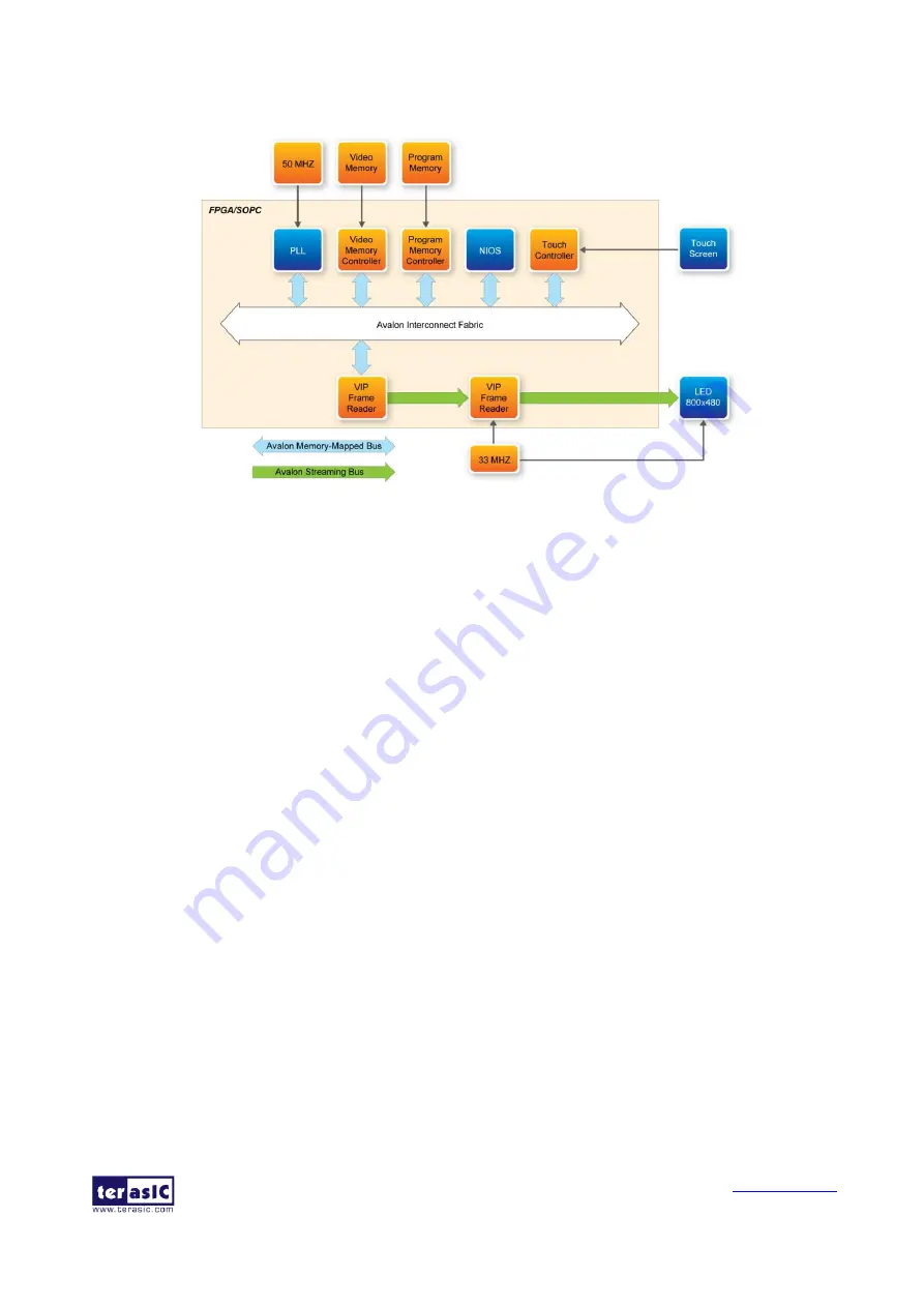
Figure 4-1 Block Diagram of the Painter Demonstration 


Demonstration Source Code 


Project directory: Painter 


Bit stream used: Painter.sof 


Nios II Workspace: Painter \Software 


Demonstration Batch File 

Demo Batch File Folder: Painter \demo_batch 

The demo batch file includes the following files: 


Batch File: test.bat, test_bashrc 


FPGA Configuration File: Painter.sof 


Nios II Program: Painter.elf 


Demonstration Setup 

1.


Make sure Quartus II and Nios II are installed on your PC 

2.


Power on the DE2-115 board 

3.


Connect USB-Blaster to the DE2-115 board and install USB-Blaster driver if necessary 

4.


Execute the demo batch file “test.bat” under the batch file folder,    Painter \demo_batch 

5.


After Nios II program is downloaded and executed successfully, you will see a painter GUI in 
the LCD

Figure 4-2


shows the GUI of the Painter Demo.


The GUI is classified into three areas: Palette, Canvas, and Gesture. Users can select pen color 
from  the  color  palette  and  start  painting  in  the  Canvas  area.  If  gesture  is  detected,  the 
associated  gesture  symbol  is  shown  in  the  gesture  area.  To  clear  canvas  content,  press  the 

Summary of Contents for MTLC

Page 1: ...1 ...

Page 2: ...HAPTER 3 USING MTLC 13 3 1 Using the 7 LCD Capacitive Touch Screen 13 3 2 Using 5 Megapixel Digital Image Sensor 16 3 3 Using the Digital Accelerometer 17 3 4 Using the Ambient Light Sensor 17 3 5 Using Terasic Multi Touch IP 18 CHAPTER 4 MTLC DEMONSTRATIONS 20 4 1 System Requirements 20 4 2 Painter Demonstration 20 4 3 Picture Viewer 24 4 4 Video and Image Processing 26 4 5 Camera Application 29 ...

Page 3: ...kit contains complete reference designs and source code for camera sensing and painter demonstrations Once the MTLC is connected and preconfigured with an FPGA hardware reference design including several ready to run demonstration applications stored on the provided SD card software developers can use these reference designs as their platform to quickly architect develop and build complex embedded...

Page 4: ...26 H x0 1790 V mm Active area 154 08 H x 85 92 V mm Module size 164 9 H x 100 0 V x 5 7 D mm Surface treatment Glare Color arrangement RGB stripe Interface Digital 5 Megapixel Digital Image Sensor Superior low light performance High frame rate Low dark current Global reset release which starts the exposure of all rows simultaneously Bulb exposure mode for arbitrary exposure times Snapshot mode to ...

Page 5: ...meter Up to 13 bit resolution at 16g SPI 3 and 4 wire digital interface Flexible interrupts modes Ambient Light Sensor Approximates human eye response Precise luminance measurement under diverse lighting conditions Programmable interrupt function with user defined upper and lower threshold settings 16 bit digital output with I2 C fast mode at 400 kHz Programmable analog gain and integration time 5...

Page 6: ...nse file is located at MTLC System CD License license_multi_touch dat There are two ways to install the license The first one is to add the license file license_multi_touch dat to the License file listed in Quartus II as shown in Figure 1 3 In order to reach this window please navigate through to Quartus II Tools License Setup Figure 1 3 License Setup The second way is to add license content to th...

Page 7: ...the Quartus II license file 1 1 3 3 A As ss se em mb bl ly y o of f M MT TL LC C o on nt to o B Bo oa ar rd ds s w wi it th h H HS SM MC C C Co on nn ne ec ct to or rs s In this section we would like to introduce how to successfully install the MTLC daughter card to FPGA boards that are equipped with HSMC connectors on top Figure 1 5 Fixed components in a MTLC kit Inside every MTLC kit package the...

Page 8: ...he host board and the HSMC cable Install the copper pillars and nuts on the mounting holes as shown in Figure 1 7 Figure 1 7 Install copper pillars and nuts on the mounting hole The HSMC cable should be already connected to the MTLC right out of the box User only needs to connect the HSMC cable to the HSMC connector on the host board as shown in Figure 1 8 ...

Page 9: ...e screws through the HSMC cable and the copper pillar as shown in Figure 1 9 Figure 1 9 Fasten screws through the HSMC cable to the copper pillars 1 1 4 4 C Co on nn ne ec ct ti iv vi it ty y Here we provide examples of MTLC being connected to different FPGA development boards Arrow s SoCKit TR4 DE2 115 and Altera Cyclone V SoC FPGA development board C5SoC ...

Page 10: ...MTLC User Manual 8 www terasic com May 22 2014 Figure 1 10 MTLC Connect C5S Figure 1 11 MTLC Connect TR4 Figure 1 12 MTLC Connect DE2 115 ...

Page 11: ...terasic com May 22 2014 Figure 1 13 MTLC Connect C5SOC 1 1 5 5 G Ge et tt ti in ng g H He el lp p Here is the contact information if you encounter any problem Terasic Technologies Tel 886 3 575 0880 Email support terasic com ...

Page 12: ...eatures of this module are listed as follows 800x480 pixel resolution LCD with 24 bit color depth Single touch and two point multi gesture support 5 Megapixel Digital Image Sensor Digital Accelerometer Ambient Light Sensor 2 2 2 2 L La ay yo ou ut t a an nd d C Co om mp po on ne en nt ts s The picture of the MTLC is shown in Figure 2 1 and Figure 2 2 It depicts the layout of the board and indicate...

Page 13: ...re 2 1 MTLC PCB and Component Diagram Top Figure 2 2 MTLC PCB and Component Diagram Bottom 2 2 3 3 B Bl lo oc ck k D Di ia ag gr ra am m o of f t th he e M MT TL LC C Figure 2 3 gives the block diagram of the MTLC board The HSMC connector houses all the ...

Page 14: ... the FPGA of a development kit through the HSMC cable Thus the user can configure the FPGA to implement any system design Figure 2 4 illustrates the connection for MTLC to the Terasic FPGA boards Figure 2 3 Block Diagram of MTLC Figure 2 4 Connection Diagram of MTLC Kit with Terasic FPGA boards ...

Page 15: ... parallel RGB data interface The MTLC is also equipped with a Touch controller which can read the coordinates of the touch points through a serial port interface To display images on the LCD panel correctly the RGB color data along with the data enable and clock signals must act according to the timing specification of the LCD touch panel as shown in Table 3 1 Table 3 2 gives the pin assignment in...

Page 16: ...ime Tvhd 8 ns Horizontal Period th 1 0 5 6 tCLK Horizontal Pulse Width thpw 3 0 tCLK thb t hpw 46DC LK is fixed Horizontal Back Porch thb 1 6 tCLK Horizontal Front Porch thfp 2 1 0 tCLK Horizontal Valid thd 8 0 0 tCLK Vertical Period tv 5 2 5 th Vertical Pulse Width tvpw 1 3 th tvpw tvb 23th is fixed Vertical Back Porch tvb 1 0 th Vertical Front Porch tvfp 2 2 th Vertical Valid tvd 480 th D A T A ...

Page 17: ...2 2 5V LCD_G3 N25 LCD green data bus bit 3 2 5V LCD_G4 L22 LCD green data bus bit 4 2 5V LCD_G5 L21 LCD green data bus bit 5 2 5V LCD_G6 U26 LCD green data bus bit 6 2 5V LCD_G7 U25 LCD green data bus bit 7 2 5V LCD_HSD U22 Horizontal sync input 2 5V LCD_MODE L24 DE SYNC mode select 2 5V LCD_POWER_CTL M25 LCD power control 2 5V LCD_R0 V28 LCD red data bus bit 0 2 5V LCD_R1 V27 LCD red data bus bit...

Page 18: ...criptions of the image sensor module Table 3 3 Pin Assignment of the CMOS Sensor Signal Name FPGA Pin No Description I O Standard CAMERA_PIXCLK J27 Pixel clock 2 5V CAMERA_D0 F24 Pixel data bit 0 2 5V CAMERA_D1 F25 Pixel data bit 1 2 5V CAMERA_D2 D26 Pixel data bit 2 2 5V CAMERA_D3 C27 Pixel data bit 3 2 5V CAMERA_D4 F26 Pixel data bit 4 2 5V CAMERA_D5 E26 Pixel data bit 5 2 5V CAMERA_D6 G25 Pixel...

Page 19: ... F28 Chip Select 2 5V GSENSOR_ALT_ADDR K27 I2C Address Select 2 5V GSENSOR_SDA_SDI_SDI O K28 Serial Data 2 5V GSENSOR_SCL_SCLK M27 Serial Communications Clock 2 5V 3 3 4 4 U Us si in ng g t th he e A Am mb bi ie en nt t L Li ig gh ht t S Se en ns so or r The APDS 9300 is a low voltage digital ambient light sensor that converts light intensity to digital signal output capable of direct I2C communic...

Page 20: ...em reset signal to iRSTN iTRIG I2C_SCLK and IC2_SDAT pins should be connected of the TOUCH_INT_n TOUCH_I2C_SCL and TOUCH_I2C_SDA signals in the 2x20 GPIO header respectively When oREADY rises it means there is touch activity and associated information is given in the oREG_X1 oREG_Y1 oREG_X2 oREG_Y2 oREG_TOUCH_COUNT and oREG_GESTURE pins For the control application when touch activity occurs it sho...

Page 21: ...The supported gestures and IDs are shown in Table 3 7 Table 3 7 Gestures Gesture ID hex One Point Gesture North 0x10 North East 0x12 East 0x14 South East 0x16 South 0x18 South West 0x1A West 0x1C North West 0x1E Rotate Clockwise 0x28 Rotate Anti clockwise 0x29 Click 0x20 Double Click 0x22 Two Point Gesture North 0x30 North East 0x32 East 0x34 South East 0x36 South 0x38 South West 0x3A West 0x3C No...

Page 22: ...l Getting Started with Altera s DE2 115 Board tut_initialDE2 115 pdf which is available on the DE2 115 system CD Copy the entire Demonstration DE2 115 folder from the MTLC system CD to your host computer 4 4 2 2 P Pa ai in nt te er r D De em mo on ns st tr ra at ti io on n This chapter shows how to control LCD and touch controller to establish a paint demo based on SOPC Builder and Altera VIP Suit...

Page 23: ...stration Setup 1 Make sure Quartus II and Nios II are installed on your PC 2 Power on the DE2 115 board 3 Connect USB Blaster to the DE2 115 board and install USB Blaster driver if necessary 4 Execute the demo batch file test bat under the batch file folder Painter demo_batch 5 After Nios II program is downloaded and executed successfully you will see a painter GUI in the LCD Figure 4 2 shows the ...

Page 24: ...igure 4 3 shows the photo when users paint in the canvas area Figure 4 4 shows the phone when counter clockwise rotation gesture is detected Figure 4 5 shows the photo when zoom in gesture is detected Figure 4 2 GUI of Painter Demo Figure 4 3 Single Touch Painting ...

Page 25: ...ual 23 www terasic com May 22 2014 Figure 4 4 Counter clockwise Rotation Gesture Figure 4 5 Zoom in Gesture Note execute the test bat under Picture_Viewer demo_batch will automatically download the sof and elf file ...

Page 26: ...s the block diagram of this demonstration The Nios II CPU here takes a key role in the demonstration It is responsible of decoding the JPEG images and coordinates the works of all the peripherals The touch panel handling program uses the timer as a regular interrupter and periodically updates the sampled coordinates Figure 4 6 Block Diagram of the Picture Viewer Demonstration Demonstration Source ...

Page 27: ...xt image will be displayed after the delay period 8 You can control the slide show as follows Press Forward to advance Reverse to go back to previous image Play Stop to play the slide or stop it On the top corner you will see the delay period seconds You can increase or decrease the delay period by touching the or buttons The max delay is 120 seconds the min delay is 1 second and the default delay...

Page 28: ...blends multiple image streams useful for implementing text overlay and picture in picture mixing Scaler A sophisticated polyphase scaler that allows custom scaling and real time updates of both the image sizes and the scaling coefficients Deinterlacer Converts interlaced video formats to progressive video format using a motion adaptive deinterlacing algorithm Also supports bob and weave algorithms...

Page 29: ... path to system integration of the video processing data path with a NTSC or PAL video input VGA output Nios II processor for configuration and control The Video and Image Processing Suite MegaCore functions have common open Avalon ST data interfaces and Avalon Memory Mapped Avalon MM control interfaces to facilitate connection of a chain of video functions and video system modeling In addition vi...

Page 30: ...e NTSC output or PAL output Connect the VGA output of the VEEK MT to a VGA monitor both LCD and CRT type of monitors should work Load the bit stream into FPGA note Run the Nios II IDE and choose VIP Software as the workspace Click on the Run button note Press the screen of the VEEK MT and drag the video frame box will result in scaling the playing window to any size as shown in Figure 4 9 Note 1 E...

Page 31: ...E2 115 The CMOS sensor module sends the raw image data to FPGA on the DE2 115 board the FPGA on the board handles image processing part and converts the data to RGB format to display on the LCD module The I2C Sensor Configuration module is used to configure the CMOS sensor module Figure 4 11 shows the block diagram of the demonstration As soon as the configuration code is downloaded into the FPGA ...

Page 32: ...DRAM which performs as a frame buffer The Multi Port SDRAM Controller has two write ports and read ports also with 16 bit data width each The writing clock is the same as CMOS sensor pix clock and the reading clock is provided by the LCD Controller which is 33MHz Finally the LCD controller fetches the RGB data from the buffer and displays it on the LCD panel continuously Because the resolution and...

Page 33: ...ess adjustment of the image captured When SW 0 is set to Off the brightness of image will be increased as KEY 1 is pressed longer If SW 0 is set to On the brightness of image will be decreased as KEY 1 is pressed shorter User can use SW 17 to mirror image of the line However remember to press KEY 0 after toggle SW 17 Note execute the test bat under Camera demo_batch will automatically download the...

Page 34: ...o source is input through the CMOS sensor on VEEK MT which generates a digital output in RGB format A number of common video functions are performed on this input stream in the FPGA These functions include clipping chroma resampling motion adaptive deinterlacing color space conversion picture in picture mixing and polyphase scaling The input and output video interfaces on the VEEK MT are configure...

Page 35: ...by modifying the related register value being written to CMOS controller chip Figure 4 13 shows the Video and Image Processing block diagram Figure 4 13 VIP Camera Example SOPC Block Diagram Key Components Demonstration Source Code Project directory VIP_Camera Bit stream used VIP_Camera sof Nios II Workspace VIP_Camera Software Demonstration Batch File Demo Batch File Folder VIP_Camera demo_batch ...

Page 36: ...15 board to reset the circuit Press KEY 2 to stop run you can press KEY 3 again to switch back to FREE RUN mode and you should be able to see whatever the camera captures on the VGA display User can use SW 17 to mirror image of the line However remember to press KEY 0 after toggle SW 17 Press and drag the video frame box will result in scaling the playing window to any size as shown in Figure 4 14...

Page 37: ...ange of angle in the x axis and y axis is computed and shown as angle data in the LCD display The value of light sensor will change as the brightness changes around the light sensor Figure 4 15 shows the hardware system block diagram of this demonstration The system is clocked by an external 50MHz oscillator Through the internal PLL module the generated 150MHz clock is used for Nios II processor a...

Page 38: ...I program is downloaded and executed successfully a prompt message will be displayed in nios2 terminal its ADXL345 s ID e5 Tilt the VEEK MT to all directions and you will find that the angle of the accelerometer and value of light sensor will change When turning the board from 80º to 10º and from 10º to 80º in Y axis or from 10ºto 80º and from 80º to 10º in Y axis the image will invert Figure 4 16...

Page 39: ... to or ry y Version Change Log V1 0 Initial Version Preliminary 5 5 2 2 C Co op py yr ri ig gh ht t S St ta at te em me en nt t Copyright 2014 Terasic Technologies All rights reserved We will continue to provide interesting examples and labs on our MTLC webpage Please visit mtlc terasic com for more information ...

Reviews: