Terasic HAN Pilot Platform Demonstration Manual Download Page 28


HAN Pilot Platform 
Demonstration Manual


27 

www.terasic.com 

September 6, 2019


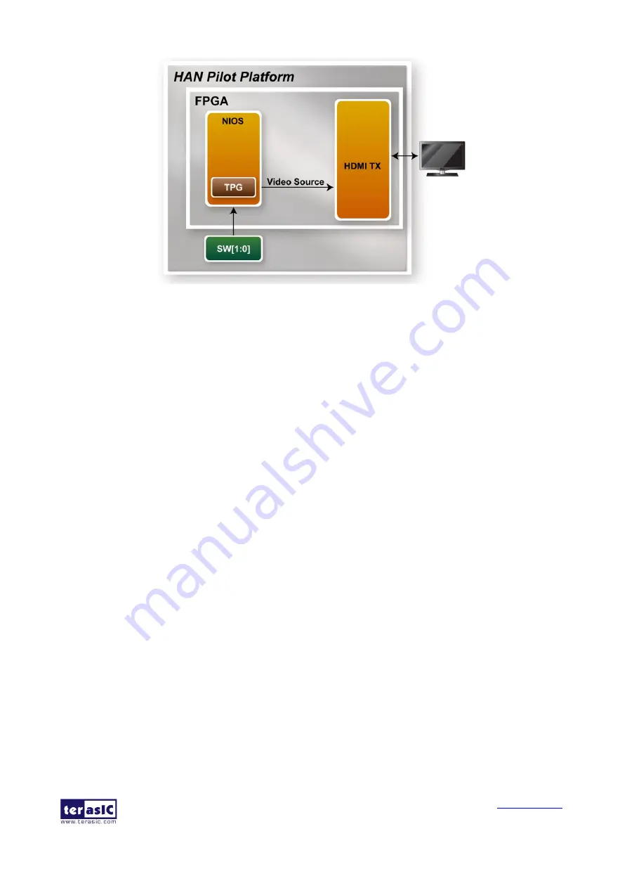
Figure 2-25 The System Block Diagram of the demonstration 


Design Tools 


Quartus Prime 18.0.0 Standard Edition 


Nios II Software Build Tools for Eclipse 18.0 


Demonstration Source Code 

Project Location: System CD\Demonstration\FPGA\HDMI_TX_4K\ 


Quartus Project directory: HDMI_TX_4K 


Nios II Eclipse: HDMI_TX_4K\software\ 


Demonstration Batch File: 

Demo Batch File Folder: HDMI_TX_4K\demo_batch\   
The demo batch file includes following files:   


Batch File for USB-Blaster II: test.bat, test.sh 


FPGA Configure File: HDMI_TX_4K.sof 


Nios II Program: vip_control.elf 


Hardware Requirement 


A PC 


An HDMI monitor capable of displaying 4K/60P 


Demonstration Setup 

1.


Make sure Quartus Prime and Nios II are installed on your PC. 

2.


Connect a HDMI monitor to the HAN Pilot Platform as shown in 

Figure 2-23

. 

3.


Connect  the  USB  Blaster  II  port  on  the  HAN  Pilot  Platform  to  the  computer  using  the  USB 
cable (do not connect the HDMI video player at this time). 

4.


Set MSEL[2:0] to 010. 

5.


Open HAN Pilot Platform power and execute demo batch file: test.bat 

Summary of Contents for HAN Pilot Platform

Page 1: ......

Page 2: ...k 18 2 7 HDMI TX and RX in 4K Resolution 22 2 8 HDMI TX in 4K Resolution 26 2 9 Low Latency Ethernet 10G MAC Demo 28 2 10 Socket Server 33 2 11 Auto Fan Speed Control 39 Chapter 3 Examples for HPS SoC...

Page 3: ...PCIe Reference Design DDR4 85 Chapter 6 PCI Express Design for Linux 92 6 1 PCI Express System Infrastructure 92 6 2 PC PCI Express Software SDK 93 6 3 PCI Express Software Stack 93 6 4 PCI Express L...

Page 4: ...categories Pure use of FPGA fabric resources Chapter 2 Pure use of HPS fabric resources Chapter 3 Use both FPGA and HPS fabric resources Chapter 4 In addition the PCIe example of HAN Pilot Platform wi...

Page 5: ...tform system CD 2 2 1 1 F Fa ac ct to or ry y D De ef fa au ul lt t C Co od de e The HAN Pilot Platform has a default configuration bit stream pre programmed which demonstrates some of the basic featu...

Page 6: ...bat FPGA Configuration File default_code sof or default_code jic Demonstration Setup 1 Make sure Quartus Prime is installed on the host PC 2 Connect HAN Pilot Platform to the host PC via USB cable Ins...

Page 7: ...temperature with the on board temperature sensor and 3 axis gyroscope 3 axis accelerometer and 3 axis magnetometer output with the on board MPU 9250 Motion Tracking device System Block Diagram Figure...

Page 8: ...tion The program provides a menu in nios terminal as shown in Figure 2 5 to provide an interactive interface With the menu users can perform the test for the temperature sensor power monitor external...

Page 9: ...he clock count in a specified period to check whether the output frequency is changed as configured For CDCM6208 programming the program can control the CDCM6208 to configure the output frequency of S...

Page 10: ...re 2 6 Temperature Demo 8 For power monitor test please input key 1 and press Enter in the nios terminal the Nios II console will display the values of voltage current and power as shown in Figure 2 7...

Page 11: ...se input key 3 and press Enter in the nios terminal first then select the desired output frequency of HDMI SFP REFCLK as shown in Figure 2 9 Figure 2 9 TXCA Demo 11 For programmable PLL TXCB test plea...

Page 12: ...c com September 6 2019 2 10 Figure 2 10 TXCB Demo 12 For programmable PLL CDCM6208 test please input key 5 and press Enter in the nios terminal first then select the desired output frequency of SATA P...

Page 13: ...at appropriate intervals System Block Diagram Figure 2 12 shows the system block diagram of this demonstration The QSYS system requires one 50 MHz and two 266 667MHz clock source The two 266 667 MHz...

Page 14: ...SDRAM When verification process is completed the result is displayed in the JTAG Terminal Design Tools Quartus Prime 18 0 0 Standard Edition Nios II Software Build Tools for Eclipse 18 0 Demonstratio...

Page 15: ...file test bat under the folder NIOS_DDR4 demo_batch 7 After Nios II program is downloaded and executed successfully a prompt message will be displayed in nios2 terminal 8 Press Key0 Key1 of the FPGA...

Page 16: ...demo_batch The demo batch file includes following files Batch File test bat FPGA Configuration File RTL_DDR4 sof Demonstration Setup 1 Make sure Quartus Prime is installed on the host PC 2 Connect HAN...

Page 17: ...gned for 4K monitor and USBC_DP_FullHD is design for Full HD Monitor If your Type C monitor only supports Full HD please use the USB_DP_FullHD for the demo setup System Block Diagram Figure 2 15 shows...

Page 18: ...Demonstration File Locations For 4K Video Output Hardware project directory USBC_DP_4K Bitstream used USBC_DP_golden_top sof Nios II Program dp_demo_test elf Demo batch file USBC_DP_4K demo_batch test...

Page 19: ...ers the data to the Slave IC FPGA by I2C in Master mode and There will be a salve I2C module in the FPGA to decode the signal and send the control signal to control the RX TX direction of the PI3USB31...

Page 20: ...www terasic com September 6 2019 Figure 2 16 Block diagram of the USBC FX3 design Demonstration Setup Hardware Setting Up as shown in Figure 2 17 Figure 2 17 USBC FX3 Demo Hardware Setting Up Design...

Page 21: ...3 demo_batch Driver win7 folder and the driver for Windows 10 is in the FPGA USBC_FX3 demo_batch Driver win10 folder Use JP6 JP5 JP4 to set the PMODE 2 0 as 0F1 F indicates floating Press KEY0 RESET F...

Page 22: ...he FX3 firmware Optional Execute the demo batch file test bat from the directory FPGA USBC_FX3 demo_batch Execute Cypress Control FPGA USBC_FX3 demo_batch Host_app download_firmware CyControl exe Use...

Page 23: ...atch the images output by the HDMI Player This demonstration supports image resolution up to 4K60P If you want to learn HDMI high performance related image processing this demo can help you learn quic...

Page 24: ...the monitor from the it s EDID and stored in the EDID RAM in the HDMI RX block The NIOS handles the control signals between the EDID and the HDMI IP in this demo The HDMI Video player is then connect...

Page 25: ...irectory HDMI_RX_TX quartus Nios II Eclipse HDMI_RX_TX software Demonstration Batch File Demo Batch File Folder HDMI_RX_TX demo_batch The demo batch file includes following files Batch File for USB Bl...

Page 26: ...ime 5 Open HAN Pilot Platform power and execute demo batch file test bat 6 Waiting for FPGA code download completed 7 First set the output resolution of the HDMI video player to 4K 60Hz and connect to...

Page 27: ...PGA This demo also has a video test pattern generator built into the FPGA The highest resolution 4K image is sent to the HDMI TX IP It is displayed via an external HDMI monitor System Block Diagram Fi...

Page 28: ...X_4K demo_batch The demo batch file includes following files Batch File for USB Blaster II test bat test sh FPGA Configure File HDMI_TX_4K sof Nios II Program vip_control elf Hardware Requirement A PC...

Page 29: ...hip between the detailed screen resolution and the switch is shown in Table 2 4 Table 2 4 Switch setting for the resolution of the test pattern SW 1 0 Resolution Setting 00 1080 60P 01 4K 60P 10 1080...

Page 30: ...ect information is shown in the Table 2 5 Table 2 5 Project Information Item Description Project Location CDROM Demonstration FPGA alt_eth FPGA Bit Stream CDROM Demonstration FPGA alt_eth output_files...

Page 31: ...the FPGA Board 5 Using Quartus to open the quartus project altera_eth_top qpf 6 Execute the demo batch file test bat under the batch file folder alt_eth demo_batch 7 Launch the System Console by sele...

Page 32: ...2 31 11 Type source show_stats tcl to checks the number of good and bad packets received as shown in Figure 2 32 12 Wait 6 minutes to complete loopback task then re type source monitor_conf tcl to se...

Page 33: ...HAN Pilot Platform Demonstration Manual 32 www terasic com September 6 2019 Figure 2 30 Ethernet 10BASE R test message for gen_conf tcl Figure 2 31 Ethernet 10BASE R test message for monitor_conf tcl...

Page 34: ...t networking protocol providing a simple cost effective option for backbone and server connectivity Gigabit Ethernet builds on top of the Ethernet protocol with speed up to 1000 Mbps or 1 gigabit per...

Page 35: ...a TCP IP port and operates the HAN Pilot Platform according to the commands from the telnet client NicheStack TCP IP stack uses the MicroC OS II RTOS multithreaded environment to provide immediate acc...

Page 36: ...ction the MDIO module is included that controls the PHY Management Module associated with the MAC block The host clock divisor is to divide the MAC control register interface clock to produce the MDC...

Page 37: ...t device is set to SGMII In this demonstration we are using SGMII MAC interface which can be configured through the management interface of the 88E1111 Ethernet device Once the link is established an...

Page 38: ...ver Nios II Eclipse Socket_Server software Nios II Project Compilation Before you attempt to compile the reference design under Nios II Eclipse make sure the project is cleaned first by clicking Clean...

Page 39: ...oaded and executed successfully a prompt message will be displayed in nios2 terminal Where the IP address and port numbers are assigned as shown below in Figure 2 38 Figure 2 38 Simple socket server 8...

Page 40: ...sion Entering a number from zero through one followed by a return causes the corresponding the LEDs LED0 LED1 to toggle on or off on the HAN Pilot Platform 2 11 Auto Fan Speed Control This demonstrati...

Page 41: ...Sensor IC TMP441 and to set the Fan Controller IC MAX6650 register for controlling the fan rotation speed Both the Temperature Sensor and the Fan Controller use the same I2C bus The Temperature Sensor...

Page 42: ...process in Figure 2 40 this module can determine the fan rotation speed value rpm and output it to the FAN_TEMP_I2C module KEY0 Which is used as system RESET function When pressing KEY0 the two modul...

Page 43: ...Pilot Platform Board Set MSEL 2 0 to 010 Power on the HAN Pilot Platform Execute the demo batch file test bat from the directory FPGA AutoFan demo_batch The fan rotation speed value is finally stabil...

Page 44: ...ntrol the two seven segments HEX 1 0 SW1 1 display the current fan rotation speed value display the thousands and the hundreds in decimal SW1 0 display the FPGA temperature value display the tens and...

Page 45: ...ctory of your choice Intel SoC EDS v18 0 is required for users to compile the c code project 3 3 1 1 U Us se er r L LE ED D a an nd d K KE EY Y Function Block Diagram Figure 3 1 shows the function blo...

Page 46: ...controls the direction of second IO pin in the associated GPIO controller and so on The value 1 in the register bit indicates the I O direction is output and the value 0 in the register bit indicates...

Page 47: ...alt_read_word read a value from a specified register alt_write_word write a value into a specified register munmap clean up memory mapping close close device driver Developers can also use the follow...

Page 48: ...r of the GPIO1 controller The status of KEY can be queried by reading the value of the bit 4 in the gpio_ext_porta register of the GPIO1 controller Figure 3 5 Gpio swporta ddr register in the GPIO1 co...

Page 49: ...nd establish connection to the UART port of Putty Type root to login into Linux 6 Type hps_gpio in the UART terminal of Putty to start the program as shown in Figure 3 6 Figure 3 6 Start the Program 7...

Page 50: ...m of USB Wi Fi dongle Wi Fi Setup Procedure 1 Connect a USB cable to the USB to UART connector J27 on the HAN Pilot Platform and the host PC 2 Connect the USB Wi Fi Dongle into the USB port on the HAN...

Page 51: ...the SSID and password for your Wi Fi AP in respectively as shown in Figure 3 10 Figure 3 10 Replace ssid and psk 9 Type ifup wlan0 in the UART terminal to connect to the Wi Fi AP as shown in Figure 3...

Page 52: ...ystem call with built in GPIO driver to implement HPS GPIO Header s loopback The built in GPIO driver is included the HAN Pilot Platform LXDE VNC Desktop BSP Function Block Diagram Figure 3 14 shows t...

Page 53: ...ameter int gpio_set_dir unsigned int gpio unsigned int out_flag The gpio_set_dir function is used to set the gpio port s data direction the parameter gpio is the port number you want to configure and...

Page 54: ...in respectively and the test data is a 32 bit value 0x1234f0f0 Described below are the loopback s implementation procedure Export gpios Set gpios s data direction Data write and read back Verify the r...

Page 55: ...nto the microSD card under the home root folder in Linux HAN Pilot Platform LXDE has pre installed this code so users can skip this copy action 4 Insert the LXDE booting micro SD card into the HAN Pil...

Page 56: ...run on SoC FPGA boards and easily communicate with other hosts via a network socket Sockets Sockets are the fundamental technology for programming software to communicate on the transport layer of net...

Page 57: ...eive information The system calls for establishing a connection which is somewhat different for the client and the server but both involve the basic construct of a socket A socket is one end of an int...

Page 58: ...ed the server is waiting for an incoming text message When a message is received it will show the receiver message on the console terminal then send the message I got your message to the client socket...

Page 59: ...based on the given hostname or IP4v Address and port number Data receiving and sending is implemented by read and write API and close is used to close the socket Figure 3 21 Socket Client Code Demonst...

Page 60: ...onnect the HAN Pilot Platform to Network via Ethernet port J25 2 Connect a USB cable to the USB to UART connector J27 on the HAN Pilot Platform and the host Windows PC 3 Copy the executable file socke...

Page 61: ...directory where socket_client exe is located 5 Then type socket_client ip address 2020 to launch the client program to connect to the host server with port number 2020 as shown in Figure 3 24 Figure 3...

Page 62: ...have the following background knowledge FPGA RTL Design Basic Quartus Prime operation skill Basic RTL coding skill Basic Qsys operation skill Knowledge about Memory Mapped Interface C Program Design B...

Page 63: ...Platform Designer should be used for the system design to add HPS component From the AXI master port of the HPS component HPS can access those Qsys components whose memory mapped slave ports are conn...

Page 64: ...r Golden Hardware Reference Design The GRD project provide by Terasic for the HAN Pilot Platform is located in the CD folder CD ROM Demonstration SOC_FPGA a10s_ghrd The project consists of the followi...

Page 65: ...B Blaster II 4 4 6 6 D De ev ve el lo op p t th he e C C C Co od de e This section introduces how to design an ARM C program to control the led_pio PIO controller SoC EDS is used to compile the C proj...

Page 66: ...e their virtual address by adding their offset relative to the peripheral region to the based virtual address virtual_base Based on the rule the virtual address of led_pio can be calculated by adding...

Page 67: ...we just need to write output value to the offset 0 register Because the led on HAN Pilot Platform is low active writing a value 0x00000003 to the offset 0 register will turn off the two LEDs Writing a...

Page 68: ...rogram will be terminated Figure 4 7 C Program for LED Shift Operation Makefile and compile Figure 4 8 shows the content of Makefile for this C project The program includes the head files provided by...

Page 69: ...e execution file hps_fpga_led to the Linux directory and type chmod x hps_fpga_led to add execution attribute to the execute file Then type hps_fpga_led to launch the ARM program The LED 1 0 on HAN Pi...

Page 70: ...A IP is used in this demonstration For detail about this IP please refer to Altera document ug_a10_pcie_avmm_dma pdf 5 5 1 1 P PC CI I E Ex xp pr re es ss s S Sy ys st te em m I In nf fr ra as st tr r...

Page 71: ...Library is implemented as a single DLL named TERASIC_PCIE_AVMM DLL This file is a 64 bit DLL With the DLL is exported to the software API users can easily communicate with the FPGA The library provide...

Page 72: ...e slot on the PC motherboard Use the PCIe cable to connect to the HAN Pilot Platform PCIE connector and the PCIe adapter card See Figure 5 3 Figure 5 3 FPGA board connect to PC 4 Power on your HAN Pil...

Page 73: ...6 2019 Figure 5 4 Screenshot of launching Update Driver Software dialog 9 In the How do you want to search for driver software dialog click Browse my computer for driver software item as shown in Fig...

Page 74: ...click the Browse button to specify the folder where altera_pcie_win_driver inf is located as shown in Figure 5 6 Click the Next button Figure 5 6 Browse for driver software on your computer 11 When th...

Page 75: ...dialog will appear as shown in Figure 5 8 Click the Close button Figure 5 8 Click Close when the installation of Altera PCI API Driver is complete 13 Once the driver is successfully installed users ca...

Page 76: ...e with the FPGA through the PCIe bus through the TERASIC_PCIE_AVMM dll API The details of API are described below 5 5 4 4 P PC CI I E Ex xp pr re es ss s L Li ib br ra ar ry y A AP PI I Below shows th...

Page 77: ...Parameters hPCIE A PCIe handle return by PCIE_Open function Return Value None PCIE_Read32 Function Read a 32 bit data from the FPGA board Prototype bool PCIE_Read32 PCIE_HANDLE hPCIE PCIE_BAR PcieBar...

Page 78: ...successful otherwise false is returned PCIE_Read8 Function Read an 8 bit data from the FPGA board Prototype bool PCIE_Read8 PCIE_HANDLE hPCIE PCIE_BAR PcieBar PCIE_ADDRESS PcieAddress uint8_t pByte Pa...

Page 79: ...GA board in DMA Maximal read size is 4GB 1 bytes Prototype bool PCIE_DmaRead PCIE_HANDLE hPCIE PCIE_LOCAL_ADDRESS LocalAddress void pBuffer uint32_t dwBufSize Parameters hPCIE A PCIe handle return by...

Page 80: ...ead PCIe Configuration Table Read a 32 bit data by given a byte offset Prototype bool PCIE_ConfigRead32 PCIE_HANDLE hPCIE uint32_t Offset uint32_t pdwData Parameters hPCIE A PCIe handle return by PCIE...

Page 81: ...e folder windows_app includes PCIE_FUNDAMENTAL exe TERASIC_PCIE_AVMM DLL Demonstration Setup 1 Set MSEL 2 0 to 010 2 Install the FPGA board on your PC as shown in Figure 5 10 Figure 5 10 FPGA board co...

Page 82: ...er 7 Goto windows_app folder execute PCIE_FUNDAMENTAL exe A menu will appear as shown in Figure 5 12 Figure 5 12 Screenshot of Program Menu 8 Type 0 followed by a ENTER key to select Led Control item...

Page 83: ...ED Control 9 Type 1 followed by an ENTER key to select Button Status Read item The button status will be report as shown in Figure 5 14 Figure 5 14 Screenshot of Button Status Report 10 Type 2 followe...

Page 84: ...ocation Quartus Project Demonstrations PCIe_Fundamental C Project Demonstrations PCIe_SW_KIT Windows PCIE_FUNDAMENTAL FPGAApplication Design Figure 5 16 shows the system block diagram in the FPGA syst...

Page 85: ...s the following major files as listed in Table 5 1 Table 5 1 Project major files NAME Description PCIE_FUNDAMENTAL cpp Main program PCIE c Implement dynamically load for TERAISC_PCIE_AVMM DLL PCIE h T...

Page 86: ...ciated bit stream file and the host is rebooted The PCI express driver is loaded successfully The LED control is implemented by calling PCIE_Write32 API as shown below The button status query is imple...

Page 87: ...t 5 Install PCIe driver if necessary 6 Restart Windows 7 Make sure the Windows has detected the FPGA Board by checking the Windows Control panel 8 Goto windows_app folder execute PCIE_DDR4 exe A menu...

Page 88: ...Pilot Platform Demonstration Manual 87 www terasic com September 6 2019 Figure 5 19 Screenshot of Program Menu Figure 5 20 Screenshot of Link Info Figure 5 21 Screenshot of On Chip Memory DMA Test Res...

Page 89: ...item The DMA write and read test result will be report as shown in Figure 5 22 Figure 5 22 Screenshot of DDR4 A SOSIMM Memory DAM Test Result 12 Type 5 followed by an ENTER key to select DMA DDR4 B Me...

Page 90: ...PGA system In the Qsys Altera PIO controller is used to control the LED and monitor the Button Status and the On Chip memory is used for performing DMA testing The PIO controllers and the On Chip memo...

Page 91: ...E_Open to open the PCI Express driver The constant DEFAULT_PCIE_VID and DEFAULT_PCIE_DID used in PCIE_Open are defined in TERASIC_PCIE_AVMM h If developer change the Vendor ID and Device ID and PCI Ex...

Page 92: ...HAN Pilot Platform Demonstration Manual 91 www terasic com September 6 2019...

Page 93: ...IP is used in this demonstration For detail about this IP please refer to Altera document ug_a10_pcie_avmm_dma pdf 6 6 1 1 P PC CI I E Ex xp pr re es ss s S Sy ys st te em m I In nf fr ra as st tr ru...

Page 94: ...nux PCIe_Driver altera_pcie_cmd h The PCI Express Library is implemented as a single so file named terasic_pcie_qsys so This file is a 64 bit library file With the library exported software API users...

Page 95: ...lease execute the steps below 1 Make sure the HAN Pilot Platform and the PC are both powered off 2 Set MSEL 2 0 to 010 3 Plug the PCIe adapter card into the PCIe slot on the PC motherboard Use the PCI...

Page 96: ...n All the files needed to create a PCIe software application are located in the directory CDROM Demonstrations PCIe_SW_KIT Linux PCIe_Library It includes the following files TERASIC_PCIE_AVMM h terasi...

Page 97: ...ero value means to ignore the vendor ID wDeviceID Specify the desired device ID A zero value means to ignore the device ID wCardIndex Specify the matched card index a zero based index based on the mat...

Page 98: ...it data Return Value Return true if read data is successful otherwise false is returned PCIE_Write32 Function Write a 32 bit data to the FPGA Board Prototype bool PCIE_Write32 PCIE_HANDLE hPCIE PCIE_B...

Page 99: ...successful otherwise false is returned PCIE_Write8 Function Write an 8 bit data to the FPGA Board Prototype bool PCIE_Write8 PCIE_HANDLE hPCIE PCIE_BAR PcieBar PCIE_ADDRESS PcieAddress uint8_t Byte P...

Page 100: ...ata retrieved from FPGA Return Value Return true if read data is successful otherwise false is returned PCIE_DmaWrite Function Write data to the memory mapped memory of FPGA board in DMA Prototype boo...

Page 101: ...e ef fe er re en nc ce e D De es si ig gn n F Fu un nd da am me en nt ta al l The application reference design shows how to implement fundamental control and data transfer in DMA In the design basic I...

Page 102: ...tus installation path export QUARTUS_ROOTDIR home centos intelFPGA 18 0 quartus 5 Execute sudo E sh test sh command to configure the FPGA 6 Restart Linux 7 Install PCIe driver The driver is located in...

Page 103: ...y to select Led Control item then input 3 hex 0x03 will make all led on as shown in Figure 6 8 If input 0 hex 0x00 all led will be turn off Figure 6 8 Screenshot of LED Control 11 Type 1 followed by a...

Page 104: ...n GNU Compiler Collection Version 4 8 is recommended Demonstration Source Code Location Quartus Project Demonstrations PCIe_Fundamental C Project Demonstrations PCIe_SW_KIT Linux PCIE_FUNDAMENTAL FPGA...

Page 105: ...ble 6 1 Table 6 1 Project major files NAME Description PCIE_FUNDAMENTAL cpp Main program PCIE c Implement dynamically load for TERAISC_PCIE_AVMM DLL PCIE h TERASIC_PCIE_AVMM h SDK library file defines...

Page 106: ...s rebooted The PCI express driver is loaded successfully The LED control is implemented by calling PCIE_Write32 API as shown below The button status query is implemented by calling the PCIE_Read32 API...

Page 107: ...tions PCIe_Fundamental demo_batch 5 Set QUARTUS_ROOTDIR variable pointing to the Quartus installation path Set QUARTUS_ROOTDIR variable by tying the following commands in terminal Replace home centos...

Page 108: ...ed by an ENTER key to select Link Info item The PCIe link information will be shown as in Figure 6 15 Gen3 link speed and x8 link width are expected Figure 6 15 Screenshot of Link Info 12 Type 3 follo...

Page 109: ...9 Figure 6 16 Screenshot of On Chip Memory DMA Test Result 13 Type 4 followed by an ENTER key to select DMA DDR4 A SODIMM Memory Test item The DMA write and read test result will be report as shown in...

Page 110: ...me 18 0 Standard Edition GNU Compiler Collection Version 4 8 is recommended Demonstration Source Code Location Quartus Project Demonstrations PCIE_DDR4 Visual C Project Demonstrations PCIe_SW_KIT Wind...

Page 111: ...TERASIC_PCIE_AVMM h SDK library file defines constant and data structure The main program PCIE_DDR4 cpp includes the header file PCIE h and defines the controller address according to the FPGA design...

Page 112: ...ero it means the driver cannot be accessed successfully In this case please make sure The FPGA is configured with the associated bit stream file and the host is rebooted The PCI express driver is load...

Page 113: ...e Logitech C310 ET USB 2760 Camera Genius WideCam F100 Audio USB Dongle Ugreen US205 These Linux BSP can be downloaded for free from the Terasic Website http HAN Pilot Platform terasic com cd 7 7 2 2...

Page 114: ...ot required press Enter UART Terminal Baud rate 115200 Data bits 8 Parity None Stop Bits 1 Flow Control no Quartus Project a10s_ghrd BSP Feature USB Audio Dongle driver USB WiFi Dongle driver Example...

Page 115: ...served DTS File Reserved 7 7 5 5 V VN NC C D De es sk kt to op p O Op pe en nC CL L B BS SP P This is a Linux BSP with VNC mode which supports Intel SDK OpenCL The Intel FPGA SDK for Open Computing La...

Page 116: ...nstration Manual 115 www terasic com September 6 2019 OpenCL Example Codes Linux Kernel Source Source https github com terasic linux socfpga tree socfpga 3 10 Branch socfpga 3 10 Under above location...

Page 117: ...hods for further technical assistance Terasic Inc 9F No 176 Sec 2 Gongdao 5th Rd East Dist Hsinchu City Taiwan 300 70 Email support terasic com Web www terasic com R Re ev vi is si io on n H Hi is st...

Reviews: