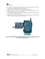


33
Margining is similar to trimming but is used for a different purpose. In that case, the rails are
intentionally set to their upper or lower limits to enable system designers to verify that their systems
work at both extremes of the voltage rail tolerances. For example, if a 5 V rail is used in the system
and specified to have an accuracy of +/- 5%, margining will set the rail to 5 V -5% to enable system
verification. Then the rail can be margined to the high side of 5 V +5% and the system verified
again. This capability exists on all four rails controlled by PSoC in this example project.
Technical Details – Other Features
Example 2 also includes two other features, typically integrated into power supervisor applications:
1.
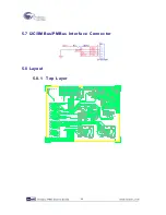
I2C/SMBus/PMBus Interface to a Host CPU. (available on the white 5-pin header on PME
EBK)
2.
EEPROM for calibration/configuration parameters, fault logging etc.
These components are both provided in the example project and are available for customization to
meet application needs. Detailed description of how to make use of those features is not currently
covered by this document. Example projects covering these topics in more detail will be added in
the future.
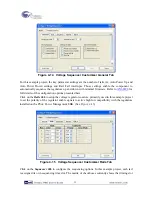
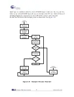
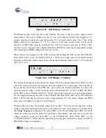
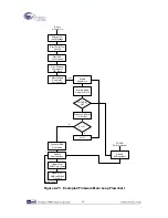
Technical Details – Firmware Flowchart
The Voltage Sequencer component, window comparator fault detection circuit and fault handling
interrupt service routine (ISR) for Example2 are identical to those described in Example1. The
additional firmware flow required for Example2 is shown in the main loop flowchart (see
Figure
4-25
). The additions to the flow are summarized below:
1.
Initialization of the PWM trim/margin hardware
2.
Initializing and starting the first ADC conversion cycle
3.
Periodically running the trim update (PWM adjust) algorithm
4.
Handling I2C/SMBus/PMBus communications
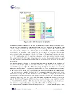
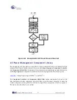
In addition to the main loop flow described above, there is an additional thread that runs
autonomously and asynchronously from the main loop. That is the ADC interrupt service routine
(ISR) thread (see
Figure 4-26
). Once the first ADC conversion is initiated by the main loop
firmware, the ADC end-of-conversion will generate an ADC ISR thread interrupt. That interrupt
will handle reading of the raw count from the ADC, filtering, conversion to absolute units (mV or
μ
A), checking voltage is within range, and then selecting the next analog input to connect to the
ADC and changing the ADC range (between 0-4096 mV and +/- 256 mV) if required.
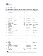
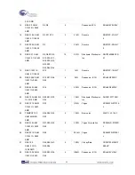
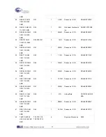
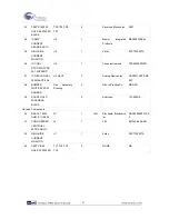
Summary of Contents for CY8CKIT-035
Page 1: ......
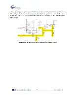
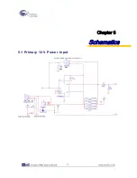
Page 38: ...Chapter 5 Schematics 5 1 Primary 12V Power Input 37 ...
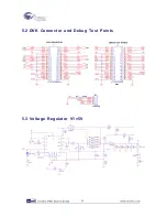
Page 39: ...5 2 DVK Connector and Debug Test Points 5 3 Voltage Regulator V1 5V 38 ...
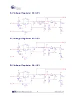
Page 40: ...5 4 Voltage Regulator V2 3 3V 5 5 Voltage Regulator V3 2 5V 5 6 Voltage Regulator V4 1 8V 39 ...
Page 41: ...5 7 I2C SMBus PMBus Interface Connector 5 8 Layout 5 8 1 Top Layer 40 ...
Page 42: ...5 8 2 Ground Layer 5 8 3 Power Layer 41 ...
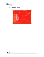
Page 43: ...5 8 4 Bottom Layer 42 ...
Page 44: ...5 8 5 Top Silkscreen 43 ...


