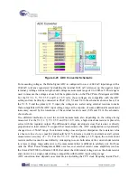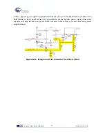
voltage. Typical power supplies respond in this manner, however for others that do not, this circuit
both internal to PSoC and external can be customized for the specific power supply chosen (for
example: inverting the PWM output such that a decrease in PWM duty cycle decreases the regulator
output voltage).
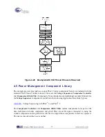
Figure 4-24 Margin and Trim Circuit for the V3=2.5 V Rail
32
Summary of Contents for CY8CKIT-035
Page 1: ......
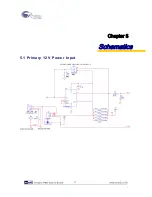
Page 38: ...Chapter 5 Schematics 5 1 Primary 12V Power Input 37 ...
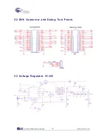
Page 39: ...5 2 DVK Connector and Debug Test Points 5 3 Voltage Regulator V1 5V 38 ...
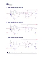
Page 40: ...5 4 Voltage Regulator V2 3 3V 5 5 Voltage Regulator V3 2 5V 5 6 Voltage Regulator V4 1 8V 39 ...
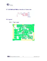
Page 41: ...5 7 I2C SMBus PMBus Interface Connector 5 8 Layout 5 8 1 Top Layer 40 ...
Page 42: ...5 8 2 Ground Layer 5 8 3 Power Layer 41 ...
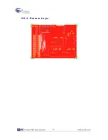
Page 43: ...5 8 4 Bottom Layer 42 ...
Page 44: ...5 8 5 Top Silkscreen 43 ...

