background image


CY8CKIT-009 PSoC 3 Processor Module 

4.


In PSoC Creator, set the appropriate example project as active by right clicking on it in the 

Workspace Explorer and selecting 

Set As Active Project


5.


In PSoC Creator, select 

Debug 

Program

 to program PSoC 

6.


Remove power from the PSoC DVK and attach the PSoC Power Management EBK to Port A 

of the PSoC DVK 

7.


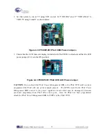
On the PSoC Power Management EBK board, make sure the power jumper (J5) is set to 

“DVK” (the default setting) 

8.


Apply 12 VDC power to the PSoC DVK 

9.


If the PME EBK cannot be detected by PSoC, status debug messages will be displayed on the 

LCD to assist with rectifying the problem 


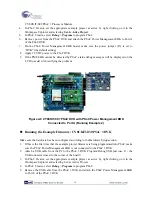
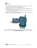
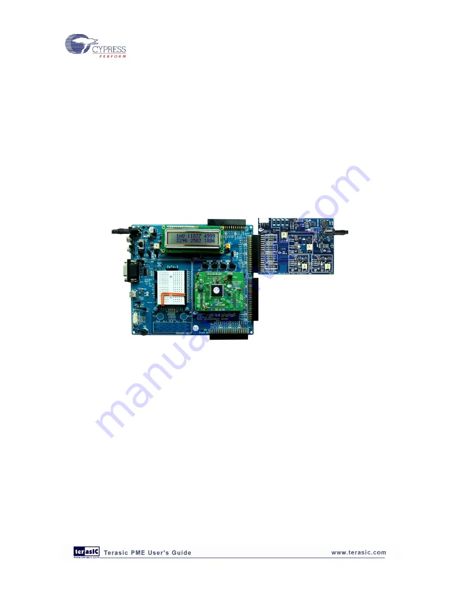
Figure 4-8 CY8CKIT-001 PSoC DVK with PSoC Power Management EBK   

Connected to Port A (Running Example 2) 

„


Running the Example Firmware: CY8CKIT-030 PSoC 3 DVK 

Make sure the hardware has been configured according to the Hardware Setup section.   
1.


If this is the first time that the example project firmware is being programmed into PSoC, make 

sure the PSoC Power Management EBK is not connected to the PSoC 3 DVK 

2.


Attach a USB cable from the PC to the PSoC 3 DVK Program/Debug USB port (use J1 - the 

USB connector closest to the corner of the board) 

3.


In PSoC Creator, set the appropriate example project as active by right clicking on it in the 

Workspace Explorer and selecting Set As Active Project 

4.


In PSoC Creator, select 

Debug 

Program

 to program PSoC 

5.


Remove the USB cable from the PSoC 3 DVK and attach the PSoC Power Management EBK 

to Port E of the PSoC 3 DVK 


18

Summary of Contents for CY8CKIT-035

Page 1: ......

Page 2: ...er 11 3 2 PME EBK Headers and Jumpers 12 3 3 Development Kit DVK Compatibility 12 CHAPTER 4 EXAMPLE PROJECTS FOR THE PME 13 4 1 Introduction 13 4 2 Software Installation 13 4 3 Hardware Setup 14 4 4 Example Projects 16 4 5 Power Management Component Library 35 4 6 Using Components in Your Own Projects 36 CHAPTER 5 SCHEMATICS 37 5 1 Primary 12V Power Input 37 5 2 DVK Connector and Debug Test Points...

Page 3: ... PMBus Interface Connector 40 5 8 Layout 40 5 8 1 Top Layer 40 5 8 2 Ground Layer 41 5 8 3 Power Layer 41 5 8 4 Bottom Layer 42 5 8 5 Top Silkscreen 43 5 9 Bill of Materials 44 CHAPTER 6 APPENDIX 48 6 1 Revision History 48 6 2 Copyright Statement 48 ...

Page 4: ...u to evaluate the system power management functions and capabilities of PSoC 3 devices You can evaluate the example projects described in this guide or design and customize your own system power management solution using components in Cypress s PSoC CreatorTM software included in this kit or by altering example projects provided with this kit The PSoC Power Management Expansion Board Kit PME EBK i...

Page 5: ...ure 1 1 PME EBK Block Diagram 1 2 About the KIT The PSoC Power Management Expansion board kit PME consists of Cypress PME EBK Quick Start Guide Power DC Adaptor 12V 2A System CD containing User s Guide this document PSoC Creator and pre requisite software PSoC Programmer and pre requisite software PME Example Firmware for the CY8CKIT 001 PSoC Development Kit Advanced Sequencer Power Supervisor 4 ...

Page 6: ...encer Power Supervisor Application Note AN62496 Voltage Sequencing with PSoC 3 and PSoC 5 Application Note AN60220 Multiplexed Comparator using PSoC 3 Datasheets for key PME EBK components Figure 1 2 shows a photograph of the PME EBK contents Figure 1 2 PME EBK Package Contents 5 ...

Page 7: ...ecisions between hardware and software allowing you to focus on what matters and getting you to market faster PSoC Creator also enables you to tap into an entire tools ecosystem with integrated compiler tool chains RTOS solutions and production programmers to support PSoC 3 1 4 Getting Help Certified as a Cypress Authorized Design Partner Terasic offers design expertise in rapidly developing PSoC ...

Page 8: ...about the architecture and block diagram of the PME EBK 2 1 Layout and Components Photos of the PME EBK are shown in Figure 2 1 and Figure 2 2 They depict the layout of the board and indicate the locations of the connectors and key components Figure 2 1 PME PCB Top 7 ...

Page 9: ...ervision to a PSoC 3 mounted on a development kit platform such as the CY8CKIT 001 PSoC Development Kit or CY8CKIT 030 PSoC 3 Development Kit PSoC 3 is not mounted on the PME EBK itself Figure 2 3 shows a high level overview of the 4 1 Power Management solution that can be implemented using the PME Up to 4 secondary regulators can be sequenced through the logic level enable outputs labeled as EN 4...

Page 10: ...t it monitors labeled as C 4 1 Note that all 5 monitored supply rail voltages are connected to both the V 4 1 and C 4 1 input pins Each voltage is connected to 2 pins to enable the hardware window comparator and the ADC with input multiplexer to run asynchronously to each other at different speeds in order to give the fastest possible fault detection time Figure 2 3 4 1 PSoC Power Management Funct...

Page 11: ... as a result Each secondary rail consists of a regulator with enable input circuitry that enables PSoC to apply a DC control voltage to the regulator feedback or adjust pin as well as fixed and adjustable potentiometer load elements Two jumpers are provided for each rail to 1 disconnect all loads or 2 disconnect only the adjustable load PME EBK provides an I2C SMBus PMBus connector A 40 pin 2 20 h...

Page 12: ...nsing Voltage Analog Ground AGND 9 10 NC Voltage Regulator 4 Fault Sensing Voltage C4 11 12 C3 Voltage Regulator 3 Fault Sensing Voltage Voltage Regulator 2 Fault Sensing Voltage C2 13 14 C1 Voltage Regulator 1 Fault Sensing Voltage Voltage Regulator 4 Trim TR4 15 16 TR3 Voltage Regulator 3 Trim Voltage Regulator 2 Trim TR2 17 18 TR1 Voltage Regulator 1 Trim Analog Ground AGND 19 20 NC Voltage Reg...

Page 13: ...he potentiometer load on V1 5V rail Installed J8 2 pin header for connecting both loads on V2 3 3V rail fixed and adjustable Installed J9 2 pin header for connecting potentiometer load on V2 3 3V rail Installed J10 2 pin header for connecting ALL loads on V3 2 5V rail fixed and adjustable Installed J11 2 pin header for connecting variable potentiometer on V3 2 5V rail Installed J12 2 pin header fo...

Page 14: ...ll the PSoC PME EBK software Insert the kit CD into the CD drive of your PC The CD is designed to auto run and the kit menu should appear See Figure 4 1 Figure 4 1 CD Autorun Kit Menu NOTE If auto run does not execute double click AutoRun on the root directory of the CD After the installation is complete the kit contents are available at the following location C Program Files Terasic PSoC Power Ma...

Page 15: ...Power Management EBK 1 0 window select Remove from the Installation Type drop down menu Follow the instructions to uninstall NOTE this method will only un install the kit software and not all the other material software that may have been installed along with the kit software 4 3 Hardware Setup The kit includes example projects for both the CY8CKIT 001 PSoC DVK and the CY8CKIT 030 PSoC 3 DVK hardw...

Page 16: ...in the ON position Figure 4 4 CY8CKIT 001 PSoC DVK LCD Power Jumper CAUTION Do not attach the PSoC Power Management EBK to the PSoC DVK until you have programmed the PSoC with one of the example projects The GPIOs routed to the PSoC Power Management EBK connect to the power regulator circuits which may be damaged if firmware previously programmed into PSoC drives those pins Once the PSoC has been ...

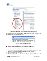
Page 17: ...rogrammed into PSoC drives those pins Once the PSoC has been programmed attach the PSoC Power Management EBK to PORT E of the PSoC 3 DVK 4 4 Example Projects The PSoC Power Management EBK includes two example projects 1 Advanced Sequencer 2 Power Supervisor The kit includes project workspaces for both the CY8CKIT 001 PSoC DVK and the CY8CKIT 030 PSoC 3 DVK To begin go to the Start Page in PSoC Cre...

Page 18: ...ew Running the Example Firmware CY8CKIT 001 PSoC DVK Make sure the hardware has been configured according to the Hardware Setup section 1 If this is the first time that the example project firmware is being programmed into PSoC make sure the PSoC Power Management EBK is not connected to the PSoC DVK 2 Apply 12 VDC power to the PSoC DVK 3 Attach the MiniProg3 first to a USB port on the PC and then ...

Page 19: ...001 PSoC DVK with PSoC Power Management EBK Connected to Port A Running Example 2 Running the Example Firmware CY8CKIT 030 PSoC 3 DVK Make sure the hardware has been configured according to the Hardware Setup section 1 If this is the first time that the example project firmware is being programmed into PSoC make sure the PSoC Power Management EBK is not connected to the PSoC 3 DVK 2 Attach a USB c...

Page 20: ...VK Program Debug USB port use J1 the USB connector closest to the corner of the board 9 If the PME EBK cannot be detected by PSoC status debug messages will be displayed on the LCD to assist with rectifying the problem 10 Going forward every time PSoC is re programmed press the Reset SW1 button on the PSoC 3 DVK to run the newly programmed firmware image Figure 4 9 CY8CKIT 030 PSoC 3 DVK with PSoC...

Page 21: ...ominal voltage If a failure occurs on any rail the rail number will be displayed next to the UV or OV indicator For example if you remove jumper J6 then you will remove power to regulators 2 through 4 This should cause an under voltage UV fault on rails 2 through 4 In that case the display should look like this see Figure 4 11 Figure 4 11 Example1 LCD Display when J6 Removed Note also that the Vol...

Page 22: ...ect the regulators on the PSoC Power Management EBK are monitored using the under voltage over voltage window comparator logic inside PSoC with programmable thresholds on each rail which generate equivalent PGOOD signals internally that connect to the Voltage Sequencer component See Figure 4 12 Figure 4 12 Advanced Sequencer Architecture To change the behavior of the sequencer double click on the ...

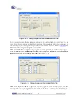
Page 23: ...configuration options presented here Click on the Rails Tab to setup the voltage regulator controls primarily used in this example project to set the polarity of the regulator enable signals to active high for compatibility with the regulators installed on the PSoC Power Management EBK See Figure 4 15 Figure 4 15 Voltage Sequencer Customizer Rails Tab Click on the Sequencer Tab to configure the se...

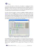
Page 24: ...should wait after enabling a regulator before checking for pass or fail on the PGOOD input The Up Delay parameter defines how long the Voltage Sequencer should wait once the timing slot has powered up successfully before moving on to the next timing slot This provides external components powered by the regulator the time needed to power up and initialize properly before moving to the next power ti...

Page 25: ...quired As the number of regulators in the systems expands the number of comparators and DACs required becomes excessive To make more efficient use of analog hardware resources an alternative implementation has been implemented based on the idea presented in Application Note AN60220 Multiplexed Comparator using PSoC 3 As shown below a single window comparator and glitch filter are rapidly time mult...

Page 26: ... the input voltage gives the best possible performance If higher speed is not required for your application and all the secondary rails in your system are lower than 4 V the maximum DAC range scaling of the regulator outputs can be eliminated Technical Details Firmware Flowchart The window comparator fault detection circuit is entirely hardware driven after it is initialized That frees the 8051 CP...

Page 27: ...s safely turned off The firmware flowchart for the Example1 project is shown below See Figure 4 19 Display LCD Intro Message Start Window Comparator H W Block Check for EBK Connection Start Voltage Sequencer Component Enable Regulator n Execute Ramp Delay for Slot n PGOOD n OK Execute Up Delay for Slot n n n 1 n 4 Handle User Interface Disable All Regulators PGOOD Failure Interrupt Reset or Power ...

Page 28: ... display something like that shown below See Figure 4 20 Figure 4 20 LCD Display Voltages The 1mV display in the top left corner indicates the units of the 4 1 power supply voltage measurements The next 2 numbers on the 1st line of the display indicate the measured 12 V primary input voltage value and the measured 5 V rail value The 2nd line of the display indicates the measured 3 3 V 2 5 V and 1 ...

Page 29: ...rrently measured by PSoC The left side of the second line shows the deviation from the nominal 5V as a percentage The right side of the second line shows the current PWM duty cycle used by the trimming hardware to achieve the currently selected voltage In this mode pressing and releasing SW1 on the CY8CKIT 001 PSoC DVK SW2 on the CY8CKIT 030 PSoC 3 DVK will trim the rail down in steps of approxima...

Page 30: ...ey will not be discussed again here One thing to note is that when running the example project on the CY8CKIT 030 PSoC 3 DVK only 2 of the voltage rails V1 5V and V3 2 5V can be routed to the window comparator circuit due to the PSoC port pins available on Port E of the DVK The other voltage rails V2 3 3V and V4 1 8V are monitored using the ADC and compared against the under over voltage threshold...

Page 31: ... on the voltage being measured For the V2 3 3 V V3 2 5 V and V4 1 8 V rails a high side shunt resistor is placed in series with the regulator output The differential voltage developed across that resistor is directly proportional to load current To support that measurement the ADC configuration is dynamically changed to a 256 mV range To minimize voltage loss and power dissipation the resistance v...

Page 32: ...uire four additional DACs to the ones already being used for the under over voltage window comparator circuit As the number of regulators in the systems expands the number of DACs required for trimming and margining becomes excessive To make more efficient use of analog hardware resources an alternative implementation has been developed based on PWM blocks with external RC filter networks to achie...

Page 33: ...not this circuit both internal to PSoC and external can be customized for the specific power supply chosen for example inverting the PWM output such that a decrease in PWM duty cycle decreases the regulator output voltage Figure 4 24 Margin and Trim Circuit for the V3 2 5 V Rail 32 ...

Page 34: ...ent Example projects covering these topics in more detail will be added in the future Technical Details Firmware Flowchart The Voltage Sequencer component window comparator fault detection circuit and fault handling interrupt service routine ISR for Example2 are identical to those described in Example1 The additional firmware flow required for Example2 is shown in the main loop flowchart see Figur...

Page 35: ...cute Ramp Delay for Slot n PGOOD n OK Execute Up Delay for Slot n n n 1 n 4 Handle User Interface Disable All Regulators PGOOD Failure Interrupt Reset or Power On n 1 Y N Y Update Trim PWM Duty Cycles Handle I2C SMBus PMBus Transfers Main Loop Start PWM Trim Circuits Start ADC Conversions Figure 4 25 Example2 Firmware Main Loop Flowchart 34 ...

Page 36: ... More information and additional example firmware for the Voltage Sequencer component is available in the following Application Note from Cypress AN62496 Voltage Sequencing with PSoC 3 and PSoC 5 The Comparator Controller and Comparator Glitch Filter custom components form part of the time multiplexed window comparator and glitch filter circuit Designers interested in using the window comparator a...

Page 37: ...pendencies Area select New Entry the file icon 3 Navigate to the KIT 035_Library cylib directory included in the example firmware distribution and select the KIT 035_Library cyprj file open or double click 4 The component library should now be included in your project Make sure that the Components and Code check boxes are checked before closing the Dependencies dialog box After adding the Componen...

Page 38: ...Chapter 5 Schematics 5 1 Primary 12V Power Input 37 ...

Page 39: ...5 2 DVK Connector and Debug Test Points 5 3 Voltage Regulator V1 5V 38 ...

Page 40: ...5 4 Voltage Regulator V2 3 3V 5 5 Voltage Regulator V3 2 5V 5 6 Voltage Regulator V4 1 8V 39 ...

Page 41: ...5 7 I2C SMBus PMBus Interface Connector 5 8 Layout 5 8 1 Top Layer 40 ...

Page 42: ...5 8 2 Ground Layer 5 8 3 Power Layer 41 ...

Page 43: ...5 8 4 Bottom Layer 42 ...

Page 44: ...5 8 5 Top Silkscreen 43 ...

Page 45: ...AP CERM 39PF 5 50V NP0 0805 C8 1 39pF 50V AVX Corporation 08055A390JAT2A 6 CAP CER 10000PF 50V 10 X7R 0805 C12 C15 C18 3 10nF 50V Murata Electronics North America GRM216R71H103 KA01D 7 DIODE SCHOTTKY 2A 20V SMB D1 1 Vishay General Semiconductor SS22 E3 52T 8 LED GREEN CLEAR 0805 SMD D2 D3 D4 D5 4 LITE ON LTST C170GKT 9 CONN HEADER R A DUAL 40POS GOLD J1 1 3M 961240 5604 AR 10 CONN HEADER 5POS 100 ...

Page 46: ...8 R59 4 2kΩ Panasonic ECG ERJ 6ENF2001V 21 RES 422 OHM 1 8W 1 0805 SMD R16 1 422Ω Panasonic ECG ERJ 6ENF4220V 22 RES 100 OHM 2W 1 2512 SMD R20 R21 R22 R24 4 100Ω Stackpole Electronics Inc RHC2512FT100R 23 RES 121K OHM 1 10W 1 0603 SMD R25 1 121kΩ Yageo RC0603FR 07121K L 24 TRIMPOT 100 OHM 6MM SQ SMD R26 R38 R52 R63 4 100Ω Bourns Inc 3361P 1 101GLF 25 RES 330 OHM 1 16W 5 0402 SMD R27 R39 R49 R60 4 ...

Page 47: ...nasonic ECG ERJ 6ENF7150V 35 RES 475K OHM 1 8W 1 0805 SMD R46 1 475kΩ Panasonic ECG ERJ 6ENF4753V 36 RES 442K OHM 1 8W 1 0805 SMD R51 1 442kΩ Panasonic ECG ERJ 6ENF4423V 37 RES 1 07K OHM 1 8W 1 0805 SMD R53 1 1 07kΩ Panasonic ECG ERJ 6ENF1071V 38 RES 340K OHM 1 8W 1 0805 SMD R57 1 340kΩ Panasonic ECG ERJ 6ENF3403V 39 RES 51 0 OHM 1 4W 1 1206 SMD R58 1 51Ω Vishay Dale CRCW120651R0F KEA 40 RES 698K ...

Page 48: ...PR 47 IC REG LDO ADJ 200MA SOT 23 6 U5 U6 U7 3 Analog Devices Inc ADP3331ARTZ RE EL7 48 BUMPER WHITE 500X 23 SQUARE See Assembly Drawing 4 Richco Plastics Co RBS 3R 49 SHUNT GOLD W HANDLE BLACK 9 Kobiconn 151 8030 E No Load Components 50 RES 1K 1 10W OHM 0 1 0805 R1 1 1kΩ Stackpole Electronics Inc RNCF0805BTC1K0 0 51 CONN HEADER VERT DUAL 40POS GOLD J4 1 3M 961240 6404 AR 52 HIGH SIDE CURRENT MONI...

Page 49: ...Chapter 6 Appendix 6 1 Revision History Version Change Log V1 0 Initial Version Final 6 2 Copyright Statement Copyright 2011 Terasic Technologies All rights reserved 48 ...

Page 50: ...Mouser Electronics Authorized Distributor Click to View Pricing Inventory Delivery Lifecycle Information Terasic P0090 ...

Reviews: