

WE865-DUAL HW User Guide
1vv0300787
Rev. 1 - 03/10/08
Reproduction forbidden without Telit Communications S.p.A. written authorization - All Rights Reserved
page 27 of 48
This transmission line shall fulfill the following requirements:
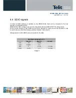
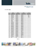
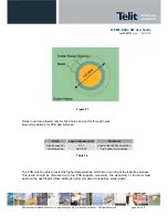
ANTENNA LINE ON PCB REQUIREMENTS
Impedance [Ohm]
50
Maximum Attenuation [dB]
0.3
Coupling with other signals is not allowed
Table 13
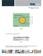
7.2 Wi-Fi antenna PCB trace guidelines
•
Ensure that the antenna line impedance is 50 ohm.
•
Keep the antenna line on the PCB as short as possible in order to limit losses.
•
Antenna line must have uniform characteristics, constant cross section, avoid meanders
and abrupt curves.
•
Keep, if possible, one layer of the PCB used only for the Ground plane.
•
Surround (on the sides, over and under) the antenna line on PCB with Ground, avoid
having other signal tracks facing directly the antenna line track.
•
The ground around the antenna line on PCB has to be strictly connected to the Ground
Plane by placing vias once per 2mm at least.
•
Place EM noisy devices as far as possible from WE865-DUAL antenna line.
•
Keep the antenna line far away from the WE865-DUAL power supply lines.
•
If you have EM noisy devices around the PCB hosting the WE865-DUAL, such as fast
switching ICs, take care of the shielding of the antenna line by burying it inside the layers
of PCB and surround it with Ground planes, or shield it with a metal frame cover.
•
If you don't have EM noisy devices around the PCB of WE865-DUAL, by using a strip-line
on the superficial copper layer for the antenna line, the line attenuation will be lower than
a buried one.


