WE865-DUAL HW User Guide
1vv0300787
Rev. 1 - 03/10/08
Reproduction forbidden without Telit Communications S.p.A. written authorization - All Rights Reserved
page 25 of 48
6 PCB layout design guidelines
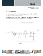
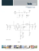
In case of implementing the input power supply circuitry as described in the previous §4.2.2, the PCB
traces connecting the switching output to the inductor and the switching diode must be as short as
possible. It is recommended to place the inductor and the diode very close to the power switching IC.
This is done in order to reduce the radiated field (noise) of the switching frequency (100-500 kHz
usually).
The use of a good common ground plane is generally suggested.
The placement of the power supply on the board should be done in such a way to guarantee that the
high current return paths in the ground plane are not overlapped to any noise sensitive lines.
The power supply input cables should be kept separate from noise sensitive lines.

