


Telecast
List of Figures
v
List of Figures
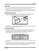
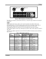
Figure 1.
Rear Panel of the Adder 882.........................................................................................1
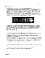
Figure 2.
Block Diagram of a One Fiber System .........................................................................2
Figure 3.
Possible Optical Configurations ...................................................................................2
Figure 4.
Installing the Rack Mount Adapters .............................................................................3
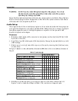
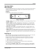
Figure 5.
Audio Setup Controls....................................................................................................5
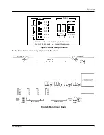
Figure 6.
Main Circuit Board .......................................................................................................5
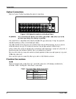
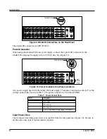
Figure 7.
ST Optical Connectors on the Rear Panel.....................................................................6
Figure 8.
XLR Connectors on the Rear Panel ..............................................................................7
Figure 9.
RS-422 D Connectors on the Rear Panel......................................................................8
Figure 10. Power Connector and Fuse Locations...........................................................................8
Figure 11. Front Panel ....................................................................................................................9
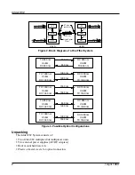
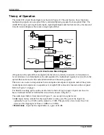
Figure 12. Electronics Block Diagram .........................................................................................10
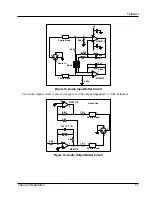
Figure 13. Audio Input Buffer Circuit..........................................................................................11
Figure 14. Audio Output Buffer Circuit.......................................................................................11
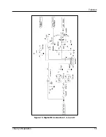
Figure 15. Digital I/O Connectors 1, 3, 5 and 7 ...........................................................................13
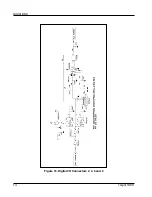
Figure 16. Digital I/O Connectors 2, 4, 6 and 8 ...........................................................................14
Figure 17. Battery Charger Block Diagram .................................................................................15
List of Tables
Table 1.
Maximum Fiber Lengths............................................................................................... 3
Table 2.
Audio Inputs.................................................................................................................. 4
Table 3.
Input and Output Cable Connections............................................................................ 6
Table 4.
Digital Cable Connections ............................................................................................ 7
Table 5.
Power Connections ....................................................................................................... 8
Table 6.
Adder 882 Main Circuits ............................................................................................ 17
Table 7.
Troubleshooting Chart ................................................................................................ 18