
Telecast
Theory of Operation
15
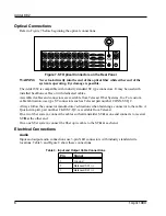
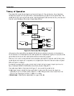
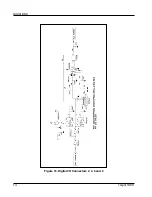
Optical
The optical output is generated from a high power LED coupled to an optical Þber. User
connections are made at a bulkhead type ST connector at the rear panel. The transmission Þber
must be matched to the Þber pigtail type speciÞed at the time of manufacture. The input uses a
pin
diode and ampliÞer to convert the optical signal back into an electrical signal. The optional single-
Þber system uses a wavelength division multiplexer to combine and then to separate the two
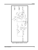
colors used. The main circuits in the Adder 882 are described in Table 6. The basic setup is
illustrated in Figure 2 on page 2.
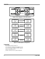
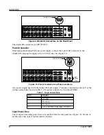
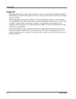
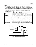
Figure 17. Battery Charger Block Diagram
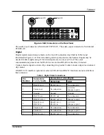
Table 6. Adder 882 Main Circuits
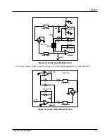
A/D
High speed analog to digital converters located in each audio channel.
Multiplexer
Sequentially presents eight RS-422 digital inputs and eight digitized audio
signals from the A/D converters to the optical output driver and four to remote
relay closures.
Demultiplexer
Takes sequential digital signals from the
pin
diode and separates them into
20 separate lines: eight to the D/A converters, eight to the RS-422 transmitters
and four to remote relay closures.
D/A
High speed digital to analog converters located in each audio channel convert
the digitized signal back to analog audio.
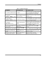
Battery charger
The battery charger (Figure 17) is active whenever an Adder 882 unit is
receiving DC power between 13.8 and 24 VDC. Charging current is limited to
a trickle level at any voltage input. Full charge takes 16 hours.
External
Power
LED
Internal
Reserve
LED
Front
Panel
Front Panel
Power Switch
Internal
Battery
+12 VDC to +24
VDC
Power to
Electronics
Charge
Control
Circuit
Rear Panel DC INPUT
1
4
Switch
Mode
Power
Supply


