background image

Maintenance—

7T1

1A

Circuit

 Board

 Pin Replacement

It is


important 

not to damage


or disturb the ferrule when 

removing the old stub of a broken pin. The ferrule is pressed 
into


the circuit board and provides a base for soldering 

the 

pin

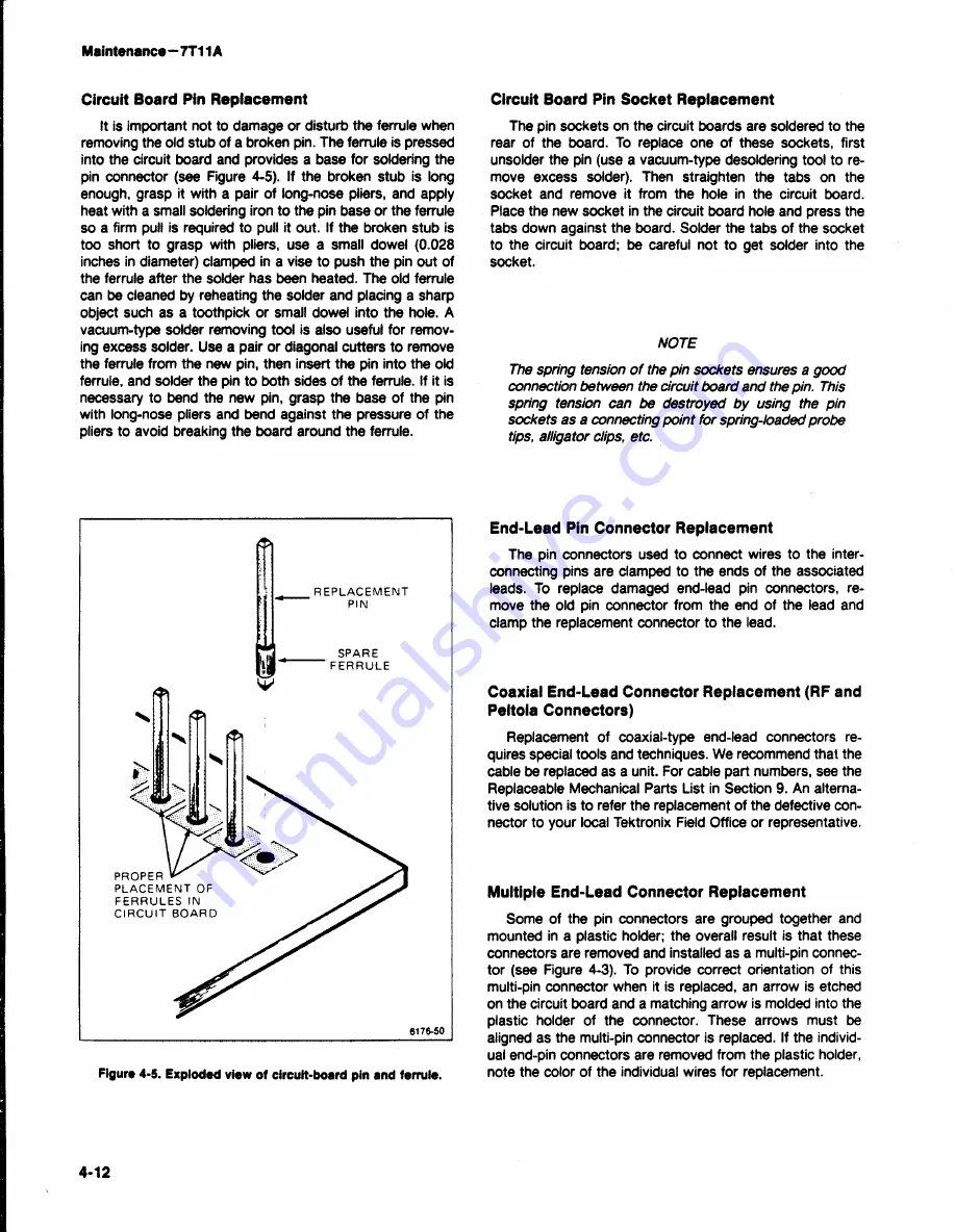
 connector (see Figure 4-5). If the broken stub is tong 

enough, 

grasp

 it with a pair of long-nose pliers, and apply 

heat


with a small soldering iron to the pin base or the ferrule 

so a firm pull is required 

to pull it out.

 If the broken stub is 

too short 

to 

grasp with pliers,

 use a small dowel (0.028 

inches 

in diameter) clamped in a vise to push the pin out of 

the


ferrule after

 the solder has been heated. The old ferrule 

can


be


cleaned by reheating the solder and placing a 

sharp 

object 

such

 as a toothpick or small dowel into the hole. A 

vacuum-type

 solder removing 

tool is also 

useful for remov­

ing


excess 

solder.

 Use a pair or diagonal cutters to remove 

the


ferrule from the new 

pin, then insert the pin into the old 

ferrule, 

and solder

 the pin to both sides of the 

ferrule. If it is 

necessary to

 bend

 the new pin, grasp the base of the pin 

with long-nose pliers and bend against the pressure of the 
pliers 

to avoid breaking 

the board around the 

ferrule.

Circuit

 Board

 Pin Socket Replacement

The

 pin 

sockets on 

the


circuit boards are soldered to the 

rear of the board. To 

replace one of these 

sockets,

 first 

unsolder

 the pin (use a vacuum-type desoldering 

tool 

to re­

move

 excess

 solder). Then straighten the tabs on the 

socket

 and remove it from the hole in the circuit board. 

Place the 

new 

socket in the circuit board hole and press the 

tabs down against the board. 

Solder the tabs of the socket 

to 

the circuit board;

 be careful not to get solder into the 

socket.

NOTE

The


spring tension of the pin sockets ensures 

a good


connection


between the circuit board

 and the pin. This


spring tension

 can be destroyed by using the pin


sockets as a connecting 

point for

 spring-loaded probe


tips, alligator clips,

 etc.

Figure

 4-5. Exploded view of circuit-board pin and ferrule.

End-Lead Pin

 Connector Replacement

The

 pin connectors used to connect wires to the

 inter­

connecting 

pins are clamped to the ends of the associated 

leads.


To replace damaged

 end-lead pin connectors, re­

move the

 old

 pin connector from the end of the lead and 

clamp 

the 

replacement connector to the lead.

Coaxial

 End-Lead Connector Replacement (RF and


Peltola

 Connectors)

Replacement


of coaxial-type end-lead

 connectors

 re­

quires

 special tools and techniques. We 

recommend that the 

cable

 be replaced as a unit. For cable part numbers, see the 

Replaceable 

Mechanical Parts List in Section 9. An alterna­

tive


solution is to refer the replacement of the defective con­

nector to your local 

Tektronix Field Office or representative.

Multiple

 End-Lead Connector Replacement

Some

 of the pin connectors are grouped together and 

mounted

 in a plastic holder; the overall result is that these 

connectors are

 removed 

and installed as a multi-pin connec­

tor 

(see 

Figure 

4-3).

 To provide

 correct orientation of this 

multi-pin 

connector 

when

 it is replaced, an arrow is etched 

on

 the circuit board and a matching arrow is molded into the 

plastic holder

 of the

 connector. These arrows must

 be 

aligned 

as 

the multi-pin connector is replaced. If the individ­

ual end-pin connectors are removed from 

the plastic holder, 

note the color of

 the 

individual wires for replacement.

4-12

Summary of Contents for 7T11A

Page 1: ...6176 00 Product Group No 42 7T11A SAMPLING SWEEP UNIT Please Check for CHANGE INFORMATION at the Rear of This Manual First Printing JUN 1986 Revised SEP 1986 Tektronix COMMTTTED TO EXCELLENCE TEK INSTRUCTION MANUAL ...

Page 2: ...price change privileges are reserved INSTRUMENT SERIAL NUMBERS Each instrument has a serial number on a panel insert tag or stamped on the chassis The first number or letter designates the country of manufacture The last five digits of the serial number are assigned sequentially and are unique to each instrument Those manufactured in the United States have six unique digits The country of manufact...

Page 3: ... Instruc tions unless qualified to do so PAGE SECTION 3 THEORY OF OPERATION Introduction 3 1 CIRCUIT THEORY 3 1 REAL TIME SAMPLING 3 1 General 3 1 Staircase Ramp Output of the Horizontal Memory 3 2 Lead Time Real Time Sampling 3 3 Samples Division Using Real Time Sampling 3 4 Summary of Real Time Basic Block Diagram 3 4 Additional Real Time Circuits 3 5 Controls Affecting Timing and Delay 3 6 Impo...

Page 4: ...2 Wiring Color Code 4 3 PAGE Resistor Color Code 4 3 Capacitor Marking 4 3 Diodes 4 3 Semiconductor Lead Configuration 4 3 Multi Pin Connector Identification 4 3 Interface Connector Pin Locations 4 3 TROUBLESHOOTING TECHNIQUES 4 6 1 Check Control Settings 4 6 2 Check Associated Test Equipment 4 6 3 Visual Check 4 6 4 Check Instrument Adjustment 4 6 5 Isolate Trouble to a Circuit 4 6 6 Check Voltag...

Page 5: ...ontrol 3 7 strobe and trigger signals 2 1 3 6 Effect of the TIME POSITION and TIME POSITION 2 2 Front panel controls connectors and indicators 2 2 controls SWEEP RANGE set at 5 ms div to 2 3 Equipment setup for Operators Checkout 10 µs div positions 3 8 Procedure 2 4 3 7 Ideal Trigger Sweep and HOMV waveform 2 4 Sequential equivalent time sampling display of relationships during real time sampling...

Page 6: ... 50 4 1 Resistor and capacitor color code 4 4 4 2 Semiconductor lead configuration 4 5 4 3 Orientation of multi pin connectors 4 6 4 4 Pin numbering on interface connector 4 6 4 5 Exploded view of circuit board pin and ferrule 4 12 FIGURE NO PAGE 4 6 Location of 200 MHz oscillator tunnel diode A3CR28 4 13 4 7 Minimum range required for the 200 MHz oscillator 4 14 4 8 Connections to switch assembli...

Page 7: ...bility to Damage from Static Discharge 4 2 4 2 Power Supply Wire Color Code 4 3 5 1 Performance Check Summary 5 3 5 2 Test Equipment 5 5 5 3 Timing 5 10 5 4 Low Frequency Triggering 5 16 5 5 Medium Frequency Triggering 5 16 5 6 High Frequency Triggering 5 16 5 7 Display Jitter with Optimum Trigger Conditions 5 20 5 8 Timing 5 37 5 9 Low Frequency Triggering 5 45 5 10 Medium Frequency Triggering 5 ...

Page 8: ...NSTRUMENT To reduce electrical shock hazard the mainframe oscilloscope chassis must be properly grounded Refer to the mainframe manual for grounding information DO NOT REMOVE INSTRUMENT COVERS To avoid electric shock hazard operating personnel must not remove the protective instrument covers Compo nent replacement and interna adjustments must be made by qualified service personnel only DO NOT OPER...

Page 9: ...iming circuit boards are a multilayer type with conductive paths laminated between the top and bottom board layers All soldering on these boards should be done with care to prevent breaking connections to the inner conductors Only experienced maintenance personnel should attempt repair of any circuit board USE PROPER CLEANING AGENTS Avoid the use of chemical cleaning agents which might damage the ...

Page 10: ...7T11A Instruction Manual 7T11A Sampling Sweep Unit viii ...

Page 11: ...ALIFIED PERSONNEL ONLY TO AVOID PERSONAL INJURY DO NOT PERFORM ANY SERVICING OTHER THAN THAT CONTAINED IN OPERATING INSTRUCTIONS UNLESS YOU ARE QUALIFIED TO DO SO REFER TO OPERATORS SAFETY SUMMARY AND SERVICE SAFETY SUMMARY PRIOR TO PERFORMING ANY SERVICE ...

Page 12: ...g permits display of the leading edge of fast rise input signals without the use of a signal delay line such as the 7M11 or a pretrigger pulse from the signal source Internal triggering or any of three modes of external trig gering can be selected by using the front panel pushbuttons A Schmitt trigger circuit is used except when HF SYNC is selected With EXT 50 Ω input selected the Schmitt circuit ...

Page 13: ...DE HORIZONTAL MODE Left Right A B 7S11 7S11 7T11 7M11 7A 7S11 7T11 7B B blank 7S11 7S11 7T11 Cl LEFT ALT ADD CHOP RIGHT X X X X X X X X X X A ALT CHOP B X X X X X X X X X X 6176 1 Figure 1 1 Several plug in configurations using the 7T11A and a 7000 series oscilloscope 1 2 A ...

Page 14: ... TIME POS RNG Within 3 beginning 25 µS after undelayed sweep start On 0 5 ms TIME POS RNG Within 3 beginning 2 5 µs after undelayed sweep start or after 500 ns from start of displayed portion of sweep Does not include 100 ns div and 200 ns div positions VARIABLE TIME DIV Range Extends fastest sweep rate to at least 4 ps div Permits increasing the speed of all sweep rates to at least 2 5 times the ...

Page 15: ...nge X1 Trig Amp 12 5 mV to 2 V P P DC to 1 GHz X10 Trig Amp 1 25 mV to 2 V P P 1 kHz to 50 MHz Safe Overload 2 V DC peak AC 1 MΩ Input Sensitivity Range X1 Trig Amp 12 5 mV to 2 V P P DC to 100 MHz X10 Trig Amp 1 25 mV to 2 V P P 1 kHz to 50 MHz Safe Overload 100 V DC or 100 V P P to 1 kHz derated 6 dB octave above 1 kHz to 5 V P P HF SYNC Input Sensitivity Range 10 mV to 500 mV peak peak at 1 GHz...

Page 16: ...nto 50 Ω Amplitude Positive going pulse of at least 400 mV Risetime 2 5 ns or less Trigger Kickout 2 mV or less into 50 Ω except HF SYNC Minimum Trigger Rate in RANDOM Mode 100 Hz SLOW RAMP GENERATOR Scan Rate REPETITIVE SCAN Continuously variable from less than 2 sweeps sec to at least 40 sweeps sec HORIZONTAL DEFLECTION SYSTEM Deflection Factor SWEEP CAL Permits adjustment of deflection factor f...

Page 17: ... Width 2 3 4 inches Length including front panel knobs and rear connector 15 inches Construction Aluminum alloy chassis with epoxy laminated circuit boards Front panel is anodized aluminum Accessories An illustrated list of the accessories supplied with the 7T11A is at the end of the Mechanical Parts List pullout pages 1 6 ...

Page 18: ...vailable NOTE Internal triggersignals are not routed through the trig ger source switches on the oscilloscope due to the frequencies involved and noise considerations Selec tion of the trigger source is made on the frontpanel of the plug ins Triggering signals travel between plug in units along 50 Ω coaxial or strip lines These signals travel between plug in units using contacts on connector strip...

Page 19: ...Operating Instructions 7T11A 6176 4 Figure 2 2 Front panel controls connectors and indicators 2 2 ...

Page 20: ... scanning of the display Scan rat is adjusted using the variable SCAN control It does not function in the three slowest real time Sweep Ranges SWEEP SWEEP OUT Jack Pin jack providing an output voltage proportional to the display With an output resistance of 10 kQ an output of one volt for each division of display is provided VARIABLE CAL IN Control When in the out position rotating the VARIABLE co...

Page 21: ...anel The remainder of the front panel contains Sweep circuit controls switches and adjustments A brief description of the function or operation of the front panel controls is provided in Figure 2 2 More detailed information is given under the heading of Detailed Operating Information Before You Begin Refer to the Change Information at the rear of this man ual for any modifications which may affect...

Page 22: ... the VARIABLE control to its fully CCW position and push it into the CAL position 7T11A TIME POSITION controls Fully clockwise SEQUENTIAL pushbutton Pushed in TIME POS RNG 5 µS TIME DIV 5 µs Div 500 ns readout VARIABLE CAL IN control Pushedin SCAN control Midposition REP pushbutton Pushedin STABILITY control Fully CCW Midposition TRIG LEVEL control SLOPE pushbutton pushed in TRIG AMP pushbutton X1...

Page 23: ...rovides a signal for triggering slightly before it delivers an output pulse to the Sampling Head input A pretrigger lead time of 75 ns is required 1 Change the settings on the following controls Pulse Generator Mode Pulse Output 7S11 mV Div 50 mV Div 3 With the TIME POSITION controls fully CW the lead ing edge of the output pulse of the pulse generator should be visible as shown in the typical dis...

Page 24: ...MATION Triggering Considerations When using Sequential equivalent time sampling to ob serve a fast risetime pulse a pretrigger or external delay line is normally required Use of a 50 Ω delay line is discussed later in this section Internal triggering or any one of three modes of External triggering can be selected by using four pushbuttons on the 7T11A front panel Triggering signals are not routed...

Page 25: ...this number is always 10 times the slowest available TIME DIV of a particular SWEEP RANGE setting The se lected TIME DIV is displayed on the CRT by the oscillo scope if the oscilloscope is provided with readout capability The VARIABLE control can provide a minimum of 2 5 to 1 magnification at any TIME DIV setting At the three slowest SWEEP RANGE settings sampling is in real time while the remainin...

Page 26: ... is removed by turning the control fully clockwise The FINE control serves the same purpose but has only about 1 as much effect as the TIME POSITION control Fig 2 7A and 2 7B show that the duration of the display or time window is ten times the selected TIME DIV setting At the SWEEP RANGE setting specified in Fig 2 7 the TIME POS RNG time positioning range is 50 µs During SE QUENTIAL operation and...

Page 27: ...been pro vided but is possible by EXT INPUT drive from a real time sweep plug in As mentioned above turning the SCAN control clock wise increases the scan rate At faster scan rates the hori zontal spacing between dots is increased Fewer samples per scan are taken resulting in a decrease in dot density Counterclockwise rotation of the SCAN control has the op posite effect scan rate decreases and do...

Page 28: ... TIME DIV settings the mode providing the best display is used The real time sampling display of 0 2 V 1 kHz square wave output of a 7000 series oscilloscope calibrator is shown in Fig 2 8 Few if any dots representing samples taken are visible during the relatively fast rise and fall time of this square wave During real time operation the dot den sity or samples per division of display is affected...

Page 29: ...ount dependent upon the selected TIME DIV setting The output of the Horizontal Amplifier is fed to the Horizontal Memory circuit The Horizontal Memory circuit provides X2 amplification of the Horizontal Amplifier output The output ramp of the Horizontal Memory differs from the usual hori zontal deflection signal in that it runs down in a series of voltage steps The output of the Horizontal Amplifi...

Page 30: ...5 volts to 5 volts is accomplished in 250 steps of 40 milli volts each Staircase Ramp Output of the Horizontal Memory Although the TTH Converter produces a linear ramp just as the time base generator in a conventional oscilloscope the ramp leaving the memory see Figure 3 4D is a stair case This is due to the sampling at regular intervals of the Horizontal Amplifier output by the Horizontal Memory ...

Page 31: ...al Time Oscillator furnishes a strobe pulse to the sampling heads in the verti cal plug ins The strobe pulse causes the sampling heads to sample the vertical input signal The amplitude of the input signal is measured at this instant when the sampling head is strobed and the signal value is stored in the vertical mem ory until the next sample is taken 20 µs later Samples are not displayed until 3 µ...

Page 32: ...ggering Vertical samples taken at these times would be displayed 13 33 53 73 and 93 µs after sweep start No fixed time relationship exists between the triggering point on the signal and the occurance of the first strobe This is en sured by frequency modulating the 50 kHz Real Time Oscil lator which determines strobe timing at an approximate 200 Hz rate Frequency specifications for the Real Time Os...

Page 33: ...ITION The block labeled Trigger in Figure 3 1 is labeled Trigger and Output TD in Figure 3 2 This block represents all cir cuits through which the triggering signal passes before ar riving at the Trigger Output tunnel diode The time at which the trigger signal causes the Trigger Output TD to fire is referred to as trigger recognition or time t0 The Trigger cir cuit switches the Start Multivibrator...

Page 34: ...operates on the Horizontal Amplifier block Essentially the TIME POSITION control de lays the start of the magnified linear sweep delivered to the Horizontal Memory Gate See Figure 3 6 Figure 3 5 shows the rate of change of the TTH Con verter output voltage for the three Real Time Sweep Ranges It should be noted that a different time scale is used in Figure 3 5 for each of the ranges The second ram...

Page 35: ...art Multivibrator which starts the negative going TTH ramp Strobe pulses are occuring at intervals of approximately 20 µs causing sampling of the vertical signal gating of the Horizontal Memory and Interdot blanking for a period of about 3 µs out of each 20 microseconds see Figure 3 4 After an interval of time determined by an RC circuit in an input to the A section of the HOMV outputs of HOMV sec...

Page 36: ... Start Multivibrator to shut off this ends the TTH ramp permits retrace blanking to operate and ends the output from the PULSE OUT connector After an interval of time 1 2 hold off interval determined by the RC previously mentioned HOMV Sections A B C and D return to their quiescent state 8 7 ms after To on Figure 3 7 The Arming and Output TD s are now returned to a ready to fire condition The next...

Page 37: ...Theory of Operation 7T11A Figure 3 7 Ideal Trigger Sweep and HOMV waveform relationships during real time sampling 3 9 ...

Page 38: ...set to the Slow Ramp Inverter input to compensate for the offset in troduced into the Horizontal Amplifier by the Time POSI TION control Unless this is done the TTH ramp could be stopped by the comparator before any change in voltage appeared at the output of the Horizontal Amplifier Slewing Comparator The purpose of the Slewing Com parator is to compare the output of the Slewing Ramp with the out...

Page 39: ...Theory of Operation 7T11A 3 11 ...

Page 40: ...ontal Memory by turning on the Memory Gate for approximately 2 µs at the 1 2 hold off time The CRT is then unblanked permitting display of a dot at a position determined by the voltages stored in the verti cal and horizontal memories After a suitable hold off inter val determined by the HOMV the circuits are returned to normal and another triggering signal can be recognized When the next trigger s...

Page 41: ...Theory of Operation 7T11A Figure 3 9 Ideal waveform relationships during sequential equivalent time sampling 3 13 ...

Page 42: ... 1 2 hold off interval the HOMV permits rearming of the Output TD to a ready for trigger condition In Figure 3 9 triggering is shown to occur again at 25 µS and the cycle repeats Since the Slow Ramp voltage is steadily rising toward its 10 volt limit the Slow Ramp volt age is slightly more positive than at the previous To and the Slewing Ramp must run more negative before the compara tor output ag...

Page 43: ...g X10 Horizontal Amplifier gain only 0 5 volts of the TTH ramp is used to produce 10 divisions of horizontal deflection In order to maintain the dot density 1000 samples sweep was assumed samples must be taken at 0 5 1000 0 5 mV intervals along the TTH ramp rundown This is accomplished by reducing the rate of change of the slow ramp at the inverter input to one tenth of its former value using the ...

Page 44: ...Theory of Operation 7T11A Figure 3 11 7T11A Blanking Logic 3 16 ...

Page 45: ...p Turn ing the Time Position control CCW increases the amount of delay between To and the start of the display window If the time between input pulses is not too long and repetition rate is constant a display can be created by triggering on one input pulse and delaying the display window so that the strobe pulses arrive at the sampling head coincident with the next input pulse Setting the triggeri...

Page 46: ... at the approximate center of the display window Ratemeter Correction The Ratemeter Correction circuit combines Lead Time Offset with the output of a compara tor This comparator is considered to be included in the Ratemeter Correction block of Figure 3 14 The comparator delivers an output if the output of the TTH Converter and the output of the Slow Ramp Inverter are unequal The error voltage from...

Page 47: ...Theory of Operation 7T11A Figure 3 14 Random mode block diagram 3 19 ...

Page 48: ...t it is also nec essary to insert an offset into the input of the Horizontal Amplifier to make it appear that the TTH Converter is putting out 0 volts instead of 2 5 volts If the TTH Con verter output level agrees with the Slow Ramp Inverter out put then the start command was correctly timed and no shift in DC correction is needed If the level is offset the start was too early Once the circuit dec...

Page 49: ... When the Trigger Output TD goes to its high level at time To a positive going pulse is fed to the To Gate of the Ratemeter When the Trigger Output TD switches back to its low level the nega tive going portion of the Ratemeter Input waveform causes reset of the Ratemeter By effectively measuring the time Figure 3 15 Ideal waveform relationships during Random equivalent time sampling 3 21 ...

Page 50: ...ampling bridge the first sample displayed is actually taken only 25 ns before To Using a slower SWEEP RANGE will provide more lead time 1 2 of time position range and permit seeing further ahead of the trigger The TIME DIV control will still permit selecting the same or other sweep rates Lack of space on Figure 3 15 prevents showing the four additional strobe pulses required to fill the ten divisi...

Page 51: ...Theory of Operation 7T11A Figure 3 17 Block diagram showing interconnections between 7T11A and vertical plug in during real time operation 3 23 ...

Page 52: ...ay K32 see Fig ure 3 18 to the Trigger Slope Amplifier Q62 and Q72 The Trigger Slope Amplifier provides the proper polarity posi tive going signal to the Schmitt Trigger circuit when trigger ing from either the positive going or negative going portion of the vertical input signal When the Schmitt Trigger circuit fires a fastrise pulse is coupled to Arming and Output tun nel diodes CR142 and CR152 ...

Page 53: ...r EXT 1 M modes With the 7T11A INT trigger pushbutton pushed in the coil of reed relay K32 is connected to 5 volts Energizing this relay completes the circuit between the sampling head and the Trigger Slope Amplifier The other set of contacts on the 7T11A INT trigger switch provide a ground to the multivibrator and trigger logic circuits in both Sampling Units Without this ground the INT trigger p...

Page 54: ... a stable source of voltage for the front panel STABILITY con trol and HF Sync Adjustment R10 The integrated circuit also delivers a stable voltage of approximately 3 volts from pin 6 for use by tunnel diode oscillator CR28 The volt age at pin 6 of the integrated circuit can be changed ap proximately 10 by rotating the STABILITY control The 200 MHz oscillator CR28 is synchronized to a sub multiple...

Page 55: ...diode oscillator During HF SYNC operation the TRIG LEVEL control functions as a fine sync control The output of CR28 is counted down by a factor of about 20 to 1 by 10 MHz tunnel diode oscillator CR29 Sync Countdown adjustment R30 is used to set the bias and fre 3 27 Figure 3 20 Simplified diegram of HF SYNC circuit ...

Page 56: ... SLOPE or Diagram 1 TRIGGER INPUT in Section 8 shows the Slope Amplifier connections with negative slope se lected Q62 and Q72 are connected as a differential ampli fier With the TRIG LEVEL control set to mid position and no input trigger current through each transistor is about 5 mA Q72 current is delivered by the 5 volt supply through CR73 while Q62 current is supplied through R69 Current throug...

Page 57: ...e tunnel diode and Q138 through resistor R132 Adjusting Trig Level Zero adjustment R120 permits the tunnel diode current to be set to just below the firing value see point 1 on Figure 3 23 A small positive going trigger signal at the emitter of Q122 causes an increase of current This increase in Q122 current flows through the tunnel diode and Q138 Even if this initial increase does not cause tunne...

Page 58: ... The four sections are shown as U110A B C and D in Figure 3 24 The four gates are divided into two sets Each set is con nected as a DC coupled multivibrator The first set is formed using the gates designated A and B and having terminals 1 2 3 4 5 and 6 These two gates form the HOMV The second set consisting of gates C and D is used for Horizon tal Memory Gate drive pulse logic and Real Time HOMV l...

Page 59: ...lied to inputs 4 and 5 of Gate B and results in 4 volts at the output pin 6 of Gate B Conduction of diode CR105 holds pin 2 positive when current through Q104 ceases shortly after trigger rec ognition To The output of Gate C is also 4 volts Pin 9 input of Gate C is above the 2 volt level if the equivalent time mode is used and below the 0 8 volt level during real time operation note voltage at top...

Page 60: ...ppens to occur simultaneous with the switching of the trigger Output tunnel diode to its high state The negative signal output of Q174 at To drives Q184 into conduction The positive pulse appearing at the collec tor of Q184 is delivered by way of Q186 to the PULSE OUT connector on the 7T11A front panel The negative pulse at the collector of Q174 occurs when Output tunnel diode CR152 switches to it...

Page 61: ...nable Real Time Retrace blanking Q164 starts conducting causing Q174 to shut off The positive pulse at the PULSE OUT connector now ends When Q174 shuts off the junction of R174 and R176 attempts to go to 50 volts but is prevented from doing so by the hold off capacitor When the charge on this capacitor reaches approximately 4 9 volts transistor Q104 con ducts returning Gates A B C and D of the HOM...

Page 62: ...Theory of Operation 7T11A Figure 3 25 Trigger Sweep and HOMV waveform relationships during real time sampling 3 34 ...

Page 63: ...Theory of Operation 7T11A Figure 3 28 Typical waveform relationships during sequential equivalent time sampling 3 35 ...

Page 64: ...f signal path providing a 5 ns delay Output tunnel diode CR152 controls the state of the tran sistor differential pair Q162 Q164 This circuit provides out put or controlling signals to a number of other circuits as shown in Figure 3 21 In order for a small trigger signal to switch the Output tunnel diode to the high state the Arming and Output tunnel diodes CR142 and CR152 respectively must first ...

Page 65: ...4 turns on Q184 also turns on rapidly This shuts off grounded base stage Q186 interrupt ing a 10 mA current Interrupting this current produces a 1 2 volt positive going output pulse into 50 Ω The output pulse is 10 volts or more if the output is open circuited Blanking Logic No blanking is possible unless Q196 is turned on Transistor Q196 will stay on as long as Q194 is shut off Transistor Q194 is...

Page 66: ...andom sampling and is discussed later in this section The second output of the TTH Converter is fed to U512A at the input of the Horizontal Amplifier Diagram 6 also discussed later in this section The TTH output ramp may be made to run positive or negative with respect to its zero volt starting point During Real Time and Sequential Sampling the TTH ramp may only run negative During Random Sampling...

Page 67: ...r does oc cur before the Ratemeter delivers a start signal to Q230 the Start Multivibrator will be turned on by the output of Q216 When Q234 turns on a negative pulse is developed at its collector The negative pulse from Q234 is fed through CR244 to the Slewing Ramp and to the gate of Q294 The negative voltage applied to the gate of Q294 shuts off Q294 permitting the Miller circuit feedback capaci...

Page 68: ...Q272 is also shut off during Random operation by the output of Q218 at the time of trigger recognition The path for Slope Drive current when developing a negative going TTH Converter output is shown in Figure 3 29 Current through Q262 results in a negative going TTH ramp at the output of the Miller circuit provided that Q294 has been shut off by the Start Multivibrator and Slope Driver Q272 is als...

Page 69: ...tput voltage will theoretically change at a rate dependent upon the value of the feedback capacitor and the input current The time t in seconds for a given change in TTH Converter output voltage can be found from the following relationship C264 acts as a temporary charge storage device preventing the input of the TTH Converter from moving until the ampli fier circuit has had a chance to operate an...

Page 70: ...is shut off and the 5 mA current is switched into the timing capacitor The parallel combination of C312 and C313 is used on the fastest sweep range 50 ns Slewing adjustment C313 sets the Slewing Ramp slope equal to that of the TTH ramp on the fastest sweep range Additional capacitance C318 is switched in on each of the three remaining equivalent time sweep ranges The same amount of capacitance is ...

Page 71: ... approximately 20 µs Memory Gate Driver Q546 applies this positive pulse to the gate of Q556 which connects the input of the Horizontal Memory Q560 to the output of the Hori zontal Amplifier for the 3 µs gating interval During real time sampling a positive going 3 µS duration pulse is also applied from the collector of Q362 to the base of Q368 This enables Q368 and provides Interdot blanking for a...

Page 72: ...ime constant is 80 µS see Figure 3 32 set by C414 and the parallel com bination of the four resistors Charging starts immediately after the network is discharged by the Reset Multivibrator The Triple Log Ramp eliminates the need to switch Rate meter capacitors when the Sweep Range setting is changed and to specify lower limits for trigger repetition rate for each Sweep Range Reset Multivibrator Th...

Page 73: ...t to the new To time interval The leadtime required to get the trace started prior to trigger recognition is provided by the signal delivered by the Start Correction circuit Q462 and Q464 If the triggering interval is very random it is possible for trigger recognition to occur part of the time prior to Pretrigger Comparator output in spite of the leadtime pro vided This presents no problems howeve...

Page 74: ...s on and a positive going pulse is coupled through CR547 to the bottom of trans former T446 primary This positive going pulse turns on Q446 and Q448 except when Q694 Diagram 7 is turned on Q694 is turned on during Slow Ramp Generator retrace time and during Sequential or Real time operation With Q694 conducting the top of T446 primary is grounded This reverse biases diode CR547 and prevents coupli...

Page 75: ... a path for offset current is provided through Q506 and R509 The direction of this current is opposite that provided by the TIME POSITION control This circuit therefore intro duces lead time offset For the 50 ns range random mode an additional offset current is provided through R507 This additional current provides the additional 50 nanoseconds of lead time needed for display of a triggering edge ...

Page 76: ...ch provides Slow Ramp Retrace blanking to the CRT and Reset Multivibrator transistors Q628 and Q626 are both off The TTH and Slewing Ramps as well as the trigger and HOMV circuits are going through their normal cycles of operation The output pulse from gate A of the HOMV Diagram 2 is applied to the base of Q628 through C630 Gate A output of the HOMV drops from approximately 4 volts to 0 volts as t...

Page 77: ... A17 Slow Ramp Retrace blanking is disabled or inhibited by turning on Q662 As previously mentioned Q662 is turned on by the negative voltage at the collector of Q626 during run up of the Slow Ramp Slow Ramp Retrace blanking is therefore prevented during this time Q662 can also be turned on disabling retrace blanking by turning on Q664 Transistor Q664 is turned on when the MAN or EXT INPUT SCAN pu...

Page 78: ...ed on the CRT Q4 and Q5 give the mainframe control over when blanking can occur by switching Q1 on and off Blanking can only occur when either of these transistors is turned on by the mainframe s control logic through interface connectors B7 of A16 This ensures that the 7T11A can only cause CRT blanking during its alloted display time MAN and EXT INPUT SCAN When the MAN or EXT INPUT is selected th...

Page 79: ...ow Ramp Genera tor is applied across R644 R646 and Dot Position Memory adjustmet R645 The 5 volt to 5 volt output of Output Amplifier U572B is applied across R647 R646 and R645 Resistors R646 and R64S provide an offset to make up for the zero level shift of the memory With no Output Amplifier error the positive going voltage from the Slow Ramp Gen erator plus the negative going voltage from U572B ...

Page 80: ...ent sent through R577 to the Slow Ramp Inverter delays firing of the Slewing Comparator Diagram 4 With firing of the Compar ator delayed the stopping of the TTH ramp and generation of the strobe pulses that cause sampling of the vertical sig nal are delayed The time or display window is therefore delayed with respect to trigger recognition With TIME POSITION control R570A set fully CCW Time Positi...

Page 81: ...DIV switch S530A cams 17 18 19 and 20 are used Another switch S531C activated when the front panel VARIABLE CAL IN knob is in the out position also provides readout logic With S531C closed a Column current of 0 2 mA and a Row current of 0 1 mA will be provided to the oscilloscope readout circuitry during time slot 3 The symbol for less than will appear on the CRT just to the left of the time per d...

Page 82: ...f 15 volts if the SWEEP RANGE control is set to an equivalent time position and an output voltage of 0 6 volts on real time positions The output of the Real Time Equivalent Time Logic cir cuit is used to enable or disable various circuits when changing from real time to equivalent time operation The notation 15 V ET 0 6 V RT is used on schematics in Section 8 Diagrams and Circuit Board Illustratio...

Page 83: ...le lubrication A lubrication kit containing the nec essary lubricants and instructions is available from Tektronix Inc Order Tektronix Part No 003 0342 02 VISUAL INSPECTION The 7T11A should be inspected occasionally for such de fects as broken connections damaged or improperly in stalled circuit boards and heat damaged parts The corrective procedure for most visible defects is obvi ous however par...

Page 84: ... physical location of components and waveform test points that appear on the respective sche matic diagrams Each circuit board illustration is arranged within a grid and has a locator index for rapid location of components contained in the corresponding schematic diagrams This instrument contains electrical components that are susceptible to damage from static discharge See Table 4 1 for relative ...

Page 85: ...ble of generating a static charge 9 Use a soldering iron that is connected to earth ground 10 Use only special antistatic suction type desoldering tools Capacitor Marking The capacitance values of common disc capactitors and small electrolytics are marked in microfarads on the side of the component body The white ceramic capacitors used in the 7T11A are color coded in picofarads using a modified E...

Page 86: ...ER pF TOLERANCE OVER 10pF UNDER 10pF BLACK 0 1 1 20 2pF 4VDC BROWN 1 10 1 10 1 0 1 pF 6VDC RED 2 102 or 100 2 102or100 2 10VDC ORANGE 3 103or 1 K 3 103 or 1000 3 15VDC YELLOW 4 104 or 10K 4 104 or 10 000 100 0 20VDC GREEN 5 105 or 100 K 1 2 105or 100 000 5 0 5pF 25VDC BLUE 6 106 or 1 M 1 4 106 or 1 000 000 35VDC VIOLET 7 1 10 107 or 10 000 000 50VDC GRAY 8 10 2 or 0 01 80 20 0 25pF WHITE 9 10 1 or...

Page 87: ...Maintenance 7T11A NOTE LEAD CONFIGURATIONS AND CASE STYLES ARE TYPICAL BUT MAY VARY DUE TO VENDOR CHANGES OR INSTRUMENT MODIFICATIONS 6176 47 Figure 4 2 Semiconductor teed configuration 4 5 ...

Page 88: ...s instrument are operating correctly Check that the signal is properly connected and that the interconnecting cables are not defective Also check the line voltage source 3 Visual Check Visually check the portion of the instrument In which the trouble is located Many problems can be located by visual indications such as unsoldered connections broken wires damaged circuit boards damaged components e...

Page 89: ...viously However be sure that circuit conditions are not such that a replacement tran sistor might also be damaged If substitute transistors are not available use a dynamic tester Static type testers are not recommended since they do not check operation under simulated operating conditions Integrated Circuits Integrated circuits can be checked with a voltmeter test oscilloscope or by direct substit...

Page 90: ...embly Tektronix Part No 012 0203 00 6 Check the Trigger Amp switch X1 No coil voltage A3Q82 input con nected to gnd X10 Voltage to X10 coil A3K80 5 V A3Q82 input connected to the trig line 7 Check the Trigger Slope switch Voltage to coil A3K71 5 V Voltage to coil A3K70 5 V Turn the power on 1 Check power supply voltages including the 10 volt reference supply provided by A2U602 8 Check operation of...

Page 91: ...own on the sche matics in Section 8 of this manual n Output Amplifiers o Dot Position Memory Once the output amplifiers have been checked reconnect the 510 Ω resistor a Pulse Out Driver When this circuit is functioning the test scope can be triggered by this pulse b Trigger Coupling Amplifiers c Start Multivibrator d Slewing Ramp It may be necessary to unplug one end of 510 Ω resistor A1R586 Set T...

Page 92: ...manufactured by Tektronix Inc To determine the manufacturer of parts refer to the cross index Manu facturer Code Number to Manufacturer at the beginning of Section 7 Replaceable Electrical Parts List and Section 9 Replaceable Mechanical Parts List Order all special parts directly from your local Tektronix Field Office or representative SOLDERING TECHNIQUES WAAN MG I To avoid electric shock and pos...

Page 93: ... Circuit Board Replacement If a circuit board is damaged beyond repair the entire assembly including all soldered on components can be re placed Part numbers are given in Section 7 Replaceable Electrical Parts List for the completely wired board Use the following procedure to remove the plug on circuit boards Metal Terminals When soldering metal terminals e g potentiometers etc use 60 40 resin cor...

Page 94: ...s down against the board Solder the tabs of the socket to the circuit board be careful not to get solder into the socket NOTE The spring tension of the pin sockets ensures a good connection between the circuit board and the pin This spring tension can be destroyed by using the pin sockets as a connecting point for spring loaded probe tips alligator clips etc Figure 4 5 Exploded view of circuit boa...

Page 95: ...quency range Adjustment of R10 is explained in detail in Section 5 of this manual The frequency change provided by the STABILITY and TRIG LEVEL controls must be at least the amount shown in Figure 4 7 If the oscillator frequency is 220 MHz with the STABILITY and TRIG LEVEL controls fully counterclock wise an oscillator frequency range of at least 55 MHz is required to ensure countdown on all frequ...

Page 96: ...Maintenance 7T11A Oscillator min freq 6176 52 Figure 4 7 Minimum range required for the 200 MHz oscillator 4 14 ...

Page 97: ...rd Then position the new contact in the hole so it is properly aligned in relation to the other switch con tacts and the mating area on the circuit board alignment tool provided in switch repair kit Finally solder the new contact into place be sure that the spring end of the contact has adequate clearance from the circuit board 7 To re install the switch assembly reverse the above procedure Pushbu...

Page 98: ... white A2R222 Black grey on white A1Q506 collector 2 Black violet ISV 2 Black Ground B A9 Random Sequential Switch circuit board assembly Lamp Connections 2 Brown orange connector A9 5V L Brown yellow A2Q734 collector Violet white R610 Scan control 2 Brown red 15 V Red white 10V Brown white A1Q60S collector Black Ground Red green on white A1Q616 Gate Blue white Ext Input Red grey on white A1R611 R...

Page 99: ...t on white A3P129 pin 2 Red orange on white A1Q714 emitter Red white A3P129 pin 3 Blue white Grey white A3P129 pin S Violet white A2R724 2 Black Ground 2 Black red connector AS 5V 2 Orange brown connector A9 5V L Red brown on white connector A14 Lamp Connections E A6 Trigger Source Switch circuit board assembly REAR Green on white connector AS F A10 Commutator Switch circuit board assembly rear vi...

Page 100: ...Red Grey on White Black Grey on White Black Red on White Rod Yellow on White Oronge White 2 Red White Violet White Red Orange Black White Brown Green on White Black Red on White Brown Blue on White Block Violet on White White Biack Green on White No Connection 2 Brawn Red 2 Block Red 2 Black Violet Grey White Black Orange on White coax Blue White Black Violet on White 6176 55 Figure 4 9 Connection...

Page 101: ...h if applicable include the instrument control settings an illustrated test setup and test equipment control settings The instrument and test equipment control settings listed in the Setup Conditions for each step may include additional settings changes from the previous step or changes to the Preliminary Control Settings making it possible to perform partial procedures The illustrated test setup ...

Page 102: ...x to locate the procedure subsec tion and the step and page number of the applicable step s Any step of a subsection can be performed separately by following the instructions given below 1 Locate the desired subsection and applicable steps e g B1 B2 etc with the Performance Check Summary table and the Performance Check Index 2 Perform the Performance Check Power Up Sequence at the start of Part I ...

Page 103: ...A6 C2 C3 C4 External 50 Ω B2 B3 B4 A2 A3 A4 A5 A6 C2 C3 C4 External 1 MΩ B2 B3 A2 A3 A4 A5 A6 C2 C3 HF Sync B4 B5 A4 A5 B10 B11 C4 C5 Display Jitter 50 Ω and 1 MΩ Sequential Mode B6 B8 C6 C8 C10 Random Mode B7 B8 C7 C8 C10 HF Sync Random or Sequential B9 C9 C10 Pulse Out Amplitude B10 C11 Risetime B10 C11 Trigger Kickout B11 C11 Minimum Trigger Rate in Random Mode B12 A2 A3 A4 A5 A6 C15 Scan Rate ...

Page 104: ...f the 7T11 A The specifications for test equipment given in Table 5 2 are the minimum required to verify Performance Re quirements Detailed operating instructions for test equip ment are omitted in these procedures Refer to the test equipment instruction manual if more information is needed If only a Performance Check is to be performed the items required for Adjustment are not required and are in...

Page 105: ...ix 7000 Series 1 mV Div to 5 V Div deflection factor 0 to 10 V or 0 1 1 MΩ input impedance Provides vertical input to the oscilloscope mainframe and internal voltage reference for comparator measurements Tektronix 7A13 6 Time Base Plug In Tektronix 7B Series Provides horizontal sweep on Oscillscope Mainframe for Differential Comparator display Tektronix 7B50A 7 Low Frequency Sine Wave Generator 50...

Page 106: ...ing Head and unit under test Tektronix Part No 015 1018 00 18 SMA to GR Adapter provided with 7T11A SMA male and GR874 connectors Provides signal interconnection between GR type cables and the unit under test Tektronix Part No 015 1007 00 19 GR to BNC Adapter four required GR874 and female BNC connectors Signal Interconnection for checking display jitter Tektronix Part No 017 0063 00 20 50 Ω BNC T...

Page 107: ...1 29 BSM to BNC Cable Coaxial 10 inches long female BSM and male BNC connectors Provides signal interconnection between Sampling Unit and unit under test for checking Pulse Out operation Tektronix Part No 012 0128 00 30 50 Ω SMA Cable two required 2 ns delay male and female SMA connectors Signal interconnection for checking HF Sync Triggering Tektronix Part No 015 1005 00 31 Patch Cord two pin jac...

Page 108: ...t temperature from 0 C to 50 C unless otherwise stated Adjustments must be performed at an ambient temperature from 20 C to 30 C for specified accuracies B TRIGGERING B1 TRIGGERING PRELIMINARY CONTROL SETTINGS 5 14 B2 CHECK LOW FREQUENCY TRIGGERING 5 15 B3 CHECK MEDIUM FREQUENCY TRIGGERING 5 15 B4 CHECK HIGH FREQUENCY TRIGGERING 5 17 B5 CHECK 12 4 GHz HF SYNC TRIGGERING 5 17 B6 CHECK SEQUENTIAL MO...

Page 109: ...n at the rear of this manual for any modifications that may affect this procedure 7T11A TIME POSITION Fully clockwise FINE Fully clockwise SLOPE TRIG LEVEL Midrange STABILITY Fully clockwise SEQUENTIAL Pushbutton Pressed in SWEEP RANGE 50µS TIME DIV 5µS VAR CAL REP Pushbutton Pressed in SCAN Midrange 3 See the TEST POINT AND ADJUSTMENT LOCA TIONS foidout page in section 8 Diagrams and Circuit Boar...

Page 110: ... longer as 7T11A SWEEP CAL is rotated between full counterclockwise and full clockwise i CHECK for the distance between time marks to in crease as the VARIABLE control is rotated clockwise and for the distance to increase at least 2 5 times the calibrated value when the control is at full clockwise see Figure 5 1 j Set 7T11A VARIABLE to calibrated operation by pressing the knob to latch it in the ...

Page 111: ...Checks and Adjustment 7T11A Part I Performance Check Figure 5 1 Typical displays for checking timing accuracy 5 11 ...

Page 112: ... µs Figura 5 2 Sweep Out waveform to check Repetitive Scan rate Test Equipment Controls Oscilloscope Mainframe Vertical Mode Left Horizontal Mode B Differential Comparator Volts Div 5 Input DC Input GND Time Base Time Div 5 6176 74 a CHECK the display for 25 ms or less per sawtooth see Figure 5 2 b Set the Time Base Time Div to 1 s and set 7T11A SCAN to full counterclockwise c CHECK the display fo...

Page 113: ...cope Mainframe Vertical Mode Right Horizontal Mode A Sampling Unit Units Div 200 Cal Variable Variable a Use the Differential Comparator Position control to center the displayed sweep Variable Full counterclockwise a CHECK for a dot on the display positioned near the right graticule edge b Set the Differential Comparator Input to DC b Press in the 7T11A EXT INPUT pushbutton Connect Sampling Unit O...

Page 114: ... Ω BNC Cable 22 GR Power Divider 23 SMA Power Divider 24 GR T Connector BEFORE YOU BEGIN 1 Perform the Performance Check Power Up Sequence 2 Refer to section 6 Instrument Options and the Change Information section at the rear of this manual for any modifications that may affect this procedure B1 TRIGGERING PRELIMINARY CONTROL SETTINGS 7T11A TIME POSITION Midrange SLOPE 3 See the TEST POINT AND ADJ...

Page 115: ...ertical deflection shown under the Display Size column Add a 10X BNC Attenuator to the 7T11A trigger signal as indicated in the right hand column of Table 5 4 Set 7T11A STABILIY and TRIG LEVEL as necessary for a stable display On real time ranges TIME POSITION also aids in stabilizing triggering Changes in control settings be tween successive steps are indicated in the table with an asterisk a CHE...

Page 116: ...IGGERING MODE SAMPLING UNIT UNITS DIV 7T11A GENERATOR FREQUENCY GENERATOR OUTPUT DISPLAY SIZE 10X ATTENUATOR SWEEP RANGE TIME DIV TRIG AMP TRIG MODE INTERNAL 50 5 µS 10 ns X10 INT 50 MHz 125 mV 2 5 div TRIGGER SIGNAL EXTERNAL 5 5 µS 10 ns X10 EXT 50 Ω 50 MHz 12 5 mV 2 5 div TRIGGER SIGNAL EXTERNAL 5 5 µS 10 ns X10 EXT 1 MΩ 50 MHz 12 5 mV 2 5 div TRIGGER SIGNAL EXTERNAL 50 5 µS 10 ns X1 EXT1 MΩ 100...

Page 117: ...quirements given in Ta ble 5 6 to obtain a stable triggered display The signal gen erator output amplitude is correct when its signal causes the amount of vertical deflection shown under the Display Size column Set 7T11A STABILIY and TRIG LEVEL as neces sary for a stable display Add BNC Attenuators to the 7T11A trigger input signal or Sampling Unit signal input as indicated in the right hand colum...

Page 118: ...pushbutton SEQUENTIAL pushbutton 50 ns 2 ns Pressed in Midrange Full clockwise Full counterclockwise Pressed in Pressed in NOTE If displayjitter exceeds the specified 10 ps value the cause may be excessive triggerjitter orjitter by other circuits in the sampling system The procedure ofstep C10 of Part ll Performance Check and Adjustment re moves the triggerportion ofdisplayjitter and is there fore...

Page 119: ... a time while using TIME POSITION STABILITY and TRIG LEVEL to maintain best possible display stability of the pulse leading edge c Set the Sampling Unit Units Div to 2 and use DC Off set and 7T11A TIME POSITION to keep the pulse leading edge visible d While maintaining best possible display stability ro tate TIME DIV to the 10 ps position e CHECK the oscilloscope display for less than 30 ps of jit...

Page 120: ...Step C10 in Part ll Performance Check and Adjustment removes the trigger portion of display jitter and is therefore a troubleshooting aid Test Equipment Controls Medium Frequency Sine Wave Generator b Disconnect the Medium Frequency Sine Wave Gen erator and connect the Low Frequency Sine Wave Genera tor in its place c CHECK the oscilloscope display for jitter using the settings and requirements gi...

Page 121: ...rmal Smooth Normal a Set the signal generator Amplitude and Sampling Unit Units Div controls to provide at least 200 mV of trigger sig nal to the 7T11A and display a steep enough waveform slope to accurately measure jitter a Rotate 7T11A TIME POSITION counterclockwise to display the rising portion of the pulse b CHECK the display for at least 400 mV of signal am plitude see Figure 5 4A b CHECK for...

Page 122: ...of the Pulse Out waveform GR TO BNC ADAPTER BNC CABLE Test Equipment Controls Sampling Unit Normal Smooth Smooth Units Div 2 DC Offset Midrange Figure 5 5 Typical display of trigger kickout a Install a Sampling Head having less than 2 mV of dis play noise in the Sampling Unit Connect the Sampling Head input to the 7T11A EXT TRIG INPUT b Set Sampling Unit DC Offset to position the trace at graticul...

Page 123: ... B12 SETUP CONDITIONS 7T11A Controls SWEEP RANGE 50 µS TIME DIV 5 µs EXT 50 Ω 2 V MAX pushbutton Pressed in TRIG LEVEL Triggered sweep Test Equipment Controls Time Mark Generator Trigger Out 10 ms a Set 7T11A TRIG LEVEL for a triggered sweep b CHECK for the displayed sweep length to be at least 9 divisions This completes the Part l Performance Check procedure 5 23 ...

Page 124: ...NG PRELIMINARY CONTROL SETTINGS 5 31 B2 EXAMINE ADJUST MEMORY GATE BLOWBY 5 32 B3 ADJUST SLEWING RAMP SERVO ZERO DOT POSITION MEMORY AND RATE SERVO ZERO 5 33 B4 EXAMINE POSITION AND SWEEP CAL RANGE 5 34 B5 EXAMINE ADJUST REAL TIME ZERO AND MEMORY GATE BAL 5 35 B6 CHECK ADJUST TIMING 5 36 B7 EXAMINE ADJUST RANDOM TIMING 5 38 B8 CHECK REPETITIVE SCAN RATE 5 39 B9 CHECK SWEEP OUT 5 39 B10 EXAMINE ADJ...

Page 125: ...e cable threaded through the Sampling Unit switch portion from the right side Tape the loose connectors to the chassis to avoid a short circuit This completes oscillator control and strobe drive circuits so the 7T11A can be operated on a plug in extender Position the EXT TRIG INPUT cable and connec tor to hang over the front of the A3 Trigger board All Exter nal Trigger inputs will still be connec...

Page 126: ...f this manual for any modifications that may affect this procedure Oscilloscope Mainframe Vertical Mode Left Horizontal Mode B 3 See the TEST POINT AND ADJUSTMENT LOCA TIONS foldout page in Section 8 Diagrams and Circuit Board Illustrations Sampling Unit NOTE The 7T11A SWEEP RANGE control and TIME POS RNG display window are integral features In this pro cedure SWEEP RANGE settings are indicated by...

Page 127: ...ns b EXAMINE the Comparator display for a reading of 10 00 volts at TP602 c ADJUST f 10 Volts adjustment R600 for 10 00 volts d Set the Differential Comparator Input and Input to GND and remove the probe tip from Test Point 602 e INTERACTION Adjustments described in this sub section may interact with other related circuits If any adjust ment is made it is recommended that the remainder of this pro...

Page 128: ... when STABILITY is set approximately 90 degrees from full counterclockwise NOTE If difficulties are encountered try performing the fol lowing step A4 and then returning to this adjustment j INTERACTION Adjustments described in this sub section may interact with other related circuits If any adjust ment is made it is recommended that the remainder of this procedure subsection be performed and the e...

Page 129: ...is procedure subsection be performed and the entire subsec tion repeated A5 EXAMINE TRIG LEVEL AND STABILITY CONTROL OPERATION NOTE If the previous step was not performed first perform step A1 A5 SETUP CONDITIONS 7T11A Controls SWEEP RANGE TIME DIV STABILITY 50 ns 1 ns Full counterclockwise SLOPE EXT 50 Ö 2 V MAX pushbutton Pressed in OSCILLOSCOPE MAINFRAME SAMP UNIT 7T11A Test Equipment Controls ...

Page 130: ...ly A3 d EXAMINE the oscilloscope display for 0 V within 2 mV use the center of the display ac component as the point of reference e ADJUST 1M Zero adjustment R45 for 0 V within 2 mV on the oscilloscope display f INTERACTION Adjustments described in this sub section may interact with other related circuits If any adjust ment is made it is recommended that the remainder of this procedure subsection ...

Page 131: ...ange Information section at the rear of this manual for any modifications that may affect this procedure 3 See the TEST POINT AND ADJUSTMENT LOCA TIONS foldout page in section 8 Diagrams and Circuit Board Illustrations B1 SCAN AND TIMING PRELIMINARY CONTROL SETTINGS 7T11A TIME POSITION Fully clockwise FINE Fully clockwise SLOPE TRIG LEVEL Midrange STABILITY Fully clockwise SEQUENTIAL Pushbutton Pr...

Page 132: ...in SCAN Midrange EXT 50 Ω 2 V MAX Pressed in SLOPE SEQUENTIAL pushbutton Pressed in c ADJUST Memory Gate Bal adjustment R550 on Timing board assembly A2 for no blowby spikes on the Differential Comparator trace d INTERACTION Adjustments described in this sub section may interact with other related circuits If any adjust ment is made it is recommended that the remainder of this procedure subsection...

Page 133: ... are not to be considered specifications d ADJUST Slewing Ramp adjustment R310 on Tim ing board assembly A2 for minimum ac and Servo Zero adjustment R588 on Logic board assembly A1 for 0 V de on the Comparator oscilloscope display center the ac waveform component on the display graticule see Figure 5 8 e Press in the 7T11A MAN pushbutton and set SCAN to full counterclockwise f ADJUST Dot Position ...

Page 134: ...n the display to be at least and 0 3 division from its initial position when 7T11A SWEEP CAL is rotated from full counterclockwise to full clockwise f Set SWEEP CAL and POSITION to their calibrated positions as described in part a Test Equipment Controls Oscilloscope Mainframe Vertical Mode Right Horizontal Mode A 6176 96 a Set front panel SWEEP CAL and POSITION for ex actly 10 divisions of range ...

Page 135: ...bly A2 to position the first time mark leading edge on or to the right of the left graticule edge while rotating 7T11A TIME DIV and SWEEP RANGE through all Real Time sweep settings 0 1 µS to 5 ms h INTERACTION To reduce interaction R555 may be adjusted at the lowest SWEEP RANGE setting and R500 adjusted while rotating the SWEEP RANGE control through the other Real Time settings Adjustments describ...

Page 136: ...o 5 ms and the Time Mark Generator to 50 µs i CHECK display for one time mark per division 3 j ADJUST Fast Timing adjustment R260 on Timing board assembly A2 for one time mark per division k Set 7T11A SWEEP RANGE to 50 ns and the Time Mark Generator to 10 ns l CHECK display for one cycle every two divisions 3 m ADJUST 50 ns Timing adjustment C292 on Timing board assembly A2 for one cycle every two...

Page 137: ... to at least 2 5 times the cali brated value when the control is at full clockwise r Set the Oscilloscope Mainframe Vertical Mode to Right and Horizontal Mode to A s CHECK timing accuracy to be within 3 by set ting 7T11A SWEEP RANGE and TIME DIV as indicated in Table 5 8 and checking for the corresponding display v Set 7T11A VARIABLE to Calibrated by pressing the knob to latch it in the CAL IN pos...

Page 138: ...be performed and the entire subsec tion repeated 7T11A Controls RANDOM pushbutton Pressed in SWEEP RANGE 5 µS TIME DIV 1 ns SCAN Full counterclockwise EXT 50 Ω 2 V MAX pushbutton Pressed in 6176 93 a Set 7T11A TRIG LEVEL to stabilize the display as much as possible NOTE These values are provided only as examples of typical instrument operation They are not to be considered specifications b EXAMINE...

Page 139: ... Input DC Input GND Time Base Time Div 5 ms Test Equipment Controls Time Base Triggering Auto AC Int Time Div 5 ms Differential Comparator Volts Div 2 Input GND a CHECK the display for 25 ms or less per sawtooth see Figure 5 11 b Set the Time Base Time Div to 1 s and set 7T11A SCAN to full counterclockwise c CHECK the display for 500 ms or more per sawtooth Figure 5 11 Sweep Out waveform to check ...

Page 140: ...terclockwise Full counterclockwise JUNCTION R34 L33 A3 TRIGGER BOARD Test Equipment Controls Differential Comparator Volts Div 20 mV BW Full Input DC Input GND Time Base Triggering Auto AC Int Time Div 05 µS Oscilloscope Mainframe Vertical Mode Left Horizontal Mode B A Teat oscilloscope display for Sync Countdown R30 adjustment a Set the Differential Comparator Position control and Time Base Posit...

Page 141: ...N Adjustments described in this sub section may interact with other related circuits If any adjust ment is made it is recommended that the remainder of this procedure subsection be performed and the entire subsec tion repeated a Set 7T11A TRIG LEVEL and STABILITY to full counterclockwise NOTE These values are provided only as examples of typical instrument operation They are not to be considered s...

Page 142: ...ols Oscilloscope Mainframe Vertical Mode Lei Horizontal Mode Sampling Unit Units Div 200 Cal Variable Variable Variable Full counterclockwise a EXAMINE the display for a dot near the right grati cule edge b Press in the 7T11A EXT INPUT pushbutton Connect theSampling Unit Offset Out to 7T11A EXT INPUT 1 V DIV 100 kΩ with a patch cord c Set Sampling Unit Offset to position the dot at the right edge ...

Page 143: ...MA Cable 2 required 25 50 Ω BNC Cable 26 50 Ω BNC Termination 27 SMA to GR Adapter 2 required 28 GR to BNC Adapter 4 required 29 GR T Connector BEFORE YOU BEGIN 1 Perform the Performance Check and Adjustment Power Up Sequence 2 Refer to section 6 Instrument Options and the Change Information section at the rear of this manual for any modifications that may affect this procedure 3 See the TEST POIN...

Page 144: ...t of vertical deflection shown under the display size column Add a 10X BNC Attenuator to the 7T11A trigger signal as indicated in the right hand column of Table 5 9 Set 7T11A STABILIY and TRIG LEVEL as necessary for a stable display On real time ranges TIME POSITION also aids in stabilizing triggering Changes in control settings be tween successive steps are indicated in the table with an asterisk...

Page 145: ...ering TRIGGERING MODE SAMPLING UNIT UNITS DIV 7T11A GENERATOR FREQUENCY GENERATOR OUTPUT DISPLAY SIZE 10X ATTENUATOR SWEEP RANGE TIME DIV TRIG AMP TRIG MODE INTERNAL 50 5 µS 10 ns X10 INT 50 MHz 125 mV 2 5 div TRIGGER SIGNAL EXTERNAL 5 5 µS 10 ns X10 EXT 50 Ω 50 MHz 12 5 mV 2 5 div TRIGGER SIGNAL EXTERNAL 5 5 µS 10 ns X10 EXT 1 MΩ 50 MHz 12 5 mV 2 5 div TRIGGER SIGNAL EXTERNAL 50 5 µS 10 ns X1 EXT...

Page 146: ...Size column Set 7T11A STABILIY and TRIG LEVEL as necessary for a stable display Add BNC Attenua tors to the 7T11A trigger input signal or Sampling Unit sig nal input as indicated in the right hand column of Table 5 11 Changes in control settings between successive steps are indicated in the table with an asterisk 7T11A Controls HF SYNC pushbutton Pressed in SWEEP RANGE 50 ns TIME DIV 10 ps Test Eq...

Page 147: ...X pushbutton Pressed in SEQUENTIAL pushbutton Pressed in Test Equipment Controls Sampling Unit Units Div Normal Smooth Pulse Generator a Set 7T11A TRIG LEVEL if necessary for a display such as that shown in Figure 5 13A b Rotate the TIME DIV control clockwise to 2 ns one step at a time while using TIME POSITION STABILITY and TRIG LEVEL to maintain best possible display stability of the pulse leadi...

Page 148: ... Test Equipment Controls No change in settings from previous step 6176 109 a Set 7T11A TRIG LEVEL if necessary for a display such as that shown in Figure 5 13A b Rotate the TIME DIV control clockwise to 2 ns one step at a time while using TIME POSITION STABILITY and TRIG LEVEL to maintain best possible display stability of the pulse leading edge c Set the Sampling Unit Units Div to 2 and use the S...

Page 149: ...rols Medium Frequency Sine Wave Generator Frequency 250 MHz Sampling Unit Units Div 50 NOTE If displayJitter exceeds the specified value the cause may be excessive triggerJitter orjitterby othercircuits in the sampling system The procedure of step C10 removes the trigger portion of display jitter and is therefore a troubleshooting aid d Disconnect the Medium Frequency Sine Wave Gen erator and conn...

Page 150: ...LITY 50 ns 2 ns Pressed in Midrange Full clockwise Full counterclockwise EXT 50 Ω 2 V MAX pushbutton Pressed in SEQUENTIAL pushbutton Pressed in BSM TO BNC CABLE Test Equipment Controls Sampling Unit Units Div 50 Normal Smooth Normal a Set the Generator Amplitude and Sampling Unit Units Div controls to provide at least 200 mV of trigger sig nal to the 7T11A and display a steep enough waveform slop...

Page 151: ...clockwise RANDOM pushbutton Pressed in TRIG AMP X1 pushbutton Pressed in SWEEP RANGE 5 µS TIME DIV 20ns INT pushbutton Pressed in REP pushbutton Pressed in BSM TO BNC CABLE Test Equipment Controls Sampling Unit Up pushbutton Pressed in DC Offset Centered display Units Div 100 Normal Smooth Normal a Rotate 7T11A TIME POSITION counterclockwise to display the rising portion of the pulse b CHECK the d...

Page 152: ...aving less than 2 mV of dis play noise in the Sampling Unit Connect the Sampling Head input to the 7T11A EXT TRIG INPUT b Set Sampling Unit DC Offset to position the trace at graticule center NOTE if the previous step was not performed first perform step C1 C13 SETUP CONDITIONS 7T11A Controls SWEEP RANGE 50 ns 50 SI BNC TERMINATION BSM TO BNC CABLE Test Equipment Controls Differential Comparator I...

Page 153: ...KBACK INTO TRIGGER NOTE If the previous step was not performed first perform step C1 C14 SETUP CONDITIONS 7T11A Controls SWEEP RANGE TIME DIV TIME POSITION Test Equipment Controls Leveled Sine wave Generator Frequency 350 kHz Oscilloscope Mainframe Vertical Mode Right Horizontal Mode A Sampling Unit Units Div 5 a Set the Sine Wave Generator amplitude and 7T11A TRIG LEVEL for a stable display with ...

Page 154: ... C15 SETUP CONDITIONS 7T11A Controls SWEEP RANGE 50 µS TIME DIV 5 µs EXT 50 0 2 V MAX pushbutton Pressed in TRIG LEVEL Triggered sweep Test Equipment Controls Time Mark Generator Trigger Out 10ms a Set 7T11A TRIG LEVEL for a triggered sweep b CHECK for the displayed sweep length to be at least 9 divisions This completes the Part ll Performance Check and Ad justment procedure 5 54 ...

Page 155: ...ECTION 6 INSTRUMENT OPTIONS No options were available for the 7T11A at the time of this printing Information about any subsequent options will be included in the CHANGE INFORMATION section at the rear of this manual 6 1 ...

Page 156: ...typical expansions are illustrated by the following Only the circuit number will appear on the diagrams and circuit board illustrations Each diagram and circuit board illustration is clearly marked with the assembly number Assembly numbers are also marked on the mechanical exploded views located in the Mechanical Parts List The component number is obtained by adding the assembly number prefix to t...

Page 157: ...94086 19396 ILLINOIS TOOL WORKS INC PAKTRON DIVISION 900 FOLLIN LANE S E VIENNA VA 22180 19701 MEPCO ELECTRA INC A NORTH AMERICAN PHILIPS CO P 0 BOX 760 MINERAL MELLS TX 76067 20932 KYOCERA INC 11620 SORRENTO VALLEY RO SAN OIEGO CD 92121 22229 SOLITRON OEVICES INC SEMICONDUCTOR GROUP SAN OIEGO OPERS 8808 BALBOA AVE SDN OIEGO CD 92123 24546 CORNING GLASS WORKS 550 HIGH ST 8RADF0RD PD 16701 24931 SP...

Page 158: ...X 5825 COMPTON CA 90224 80009 TEKTRONIX INC 4900 S M GRIFFITH OR PO B0X 500 BEAVERTON OR 97077 91418 RADIO MATERIALS CORP 4242 BYRN MAHR AVE M CHICAGO IL 60646 95275 VITRAMON INC BOX 544 BRIDGEPORT CT 06601 98291 SEALECTRO CORP 225 HOYT MAMARONECK NY 10544 TK0961 NEC ELECTRONICS USA INC 401 ELLIS ST MOUNTAIN VIEN CA 94043 TK1345 ZMAN ANO ASSOCIATES 7633 S 180TH KENT NA 98032 REV SEP 1986 7 3 ...

Page 159: ...MICOND DVC DI SW SI 30V 150MB 30V 03508 DB2527 1N4152 A1CR5 152 0322 00 SEMICOND DVC DI SCHOTTKY BARRIER SI I 15V 50434 5082 2672 A1CR591 152 0141 02 SEMICOND DVC DI SW SI 30V 150MB 30V 03508 002527 1N4152 A1CR595 152 0141 02 SEMICOND DVC DI SW SI 30V 150MB 30V 03508 002527 1N4152 A1CR596 152 0141 02 SEMICOND DVC DI SW SI 30V 150MB 30V 03508 002527 1N4152 A1CR621 152 0141 02 SEMICOND DVC 01zSM SI ...

Page 160: ...68 NTR25J E04K7 A1R504 315 0303 00 RES FXD FI LM 30 0HM 5X 0 25H 19701 5O43CX3OK0OJ A1R505 315 0563 00 RES FXD FILM 56K 0HM 5X 0 25H 19701 5043CX56KOOJ A1R571 315 0103 00 RES FXD FILM 10 0HM 5X 0 25H 19701 5O43CX10KOOJ A1R572 315 0103 00 RES FXD FILM 10K 0HM 5X 0 25H 19701 5O43CX1OK0OJ A1R576 315 0105 00 RES FXD FILM 1M 0HM 5X 0 25 19701 5043CX1MOOOJ A1R577 321 0289 00 RES FXD FILN 10 0K 0HM 1X 0 ...

Page 161: ...M 1X 0 125M TC T0 07716 CEA056201F A1R668 321 0277 00 RES FXD FILM 7 50K 0HM 1X 0 125M TC T0 24546 NA5507501F A1R669 315 0472 00 RES FXD FILM 4 7K 0HM 5X 0 25M 57668 NTR25J E04K7 A1R670 315 0103 00 RES FXD FILM 10K 0HM 5X 0 25M 19701 5043CX10KOOJ A1R671 315 0102 00 RES FXD FILM 1K 0HM 5X 0 25M 57668 NTR25JE01K0 A1R672 315 0513 00 RES FXD FILM 51K 0HM 5X 0 25M 57668 NTR25J E51K0 A1R673 321 0289 03 ...

Page 162: ...C344 283 0070 00 CAP FXD CER DI 30PF 102 50V 51642 200 050 NP0 300K A2C346 283 0121 00 CAP FXD CER DI 1000PF 202 200V 91418 5P102M2011958 A2C348 281 0762 00 CAP FXD CER DI 27PF 202 100V 04222 M0101D270MOO A2C349 281 0773 00 CAP FXD CER DI 0 01UF 102 100V 04222 M0201C103KOO A2C353 283 0253 00 CBP FXD CER DI 0 01UF 102 100V 04222 15051C103KZT6C A2C356 281 0811 00 CAP FXD CER DI 10PF 102 100V 04222 M...

Page 163: ...414 152 0141 02 SEMICOND DVC DI SW SI 30V 150MA 30V 03508 0A2527 1N4152 A2CR416 152 0141 02 SEMICOND DVC DI SW SI 30V 150MA 30V 03508 0A2527 1N4152 A2CR446 152 0141 02 SEMICOND DVC DI SW SI 30V 150MA 30V 03508 0A2527 1N4152 A2CR502 152 0141 02 SEMICOND DVC DI SW SI 30V 150MA 30V 03508 0A2527 1N4152 A2CR503 152 0141 02 SEMICOND DVC DI SW SI 30V 150MA 30V 03508 0A2527 1N4152 A2CR514 152 0071 00 SEMI...

Page 164: ...92 04713 SPS6917 A2Q512 151 0220 00 TRANSISTOR PNP SI TO 92 80009 151 0220 00 A2Q514 153 0588 00 TRANSISTOR SELECTED 80009 153 0588 00 A2Q524 153 0588 00 TRANSISTOR SELECTED 80009 153 0588 00 A2Q542 151 0164 00 TRANSISTOR PNP SI TO 92 04713 2N2907B A2Q544 151 0207 00 TRANSISTOR NPN SI X 55 SEL 57668 XD11BCP0207 A2Q546 151 0188 00 TRANSISTOR PNP SI TO 92 80009 151 0188 00 A2Q552 151 0190 00 TRANSIS...

Page 165: ... A2R286 315 0103 00 RES FXD FILM 10K OHM 5X 0 25H 19701 5043CX10K00J A2R287 321 0289 00 RES FXD FILM 10 0K OHM 1X 0 125H TOTO 19701 5033ED10K0F A2R294 315 0683 00 RE5 FXD FILM 68K OHM 5X 0 25H 57668 NTR25J E68K0 A2R296 315 0203 00 RES FXD FILM 20K OHM 5X 0 25M 57668 MTR25J E 20K A2R299 315 0622 00 RES FXD FILM 6 2K OHM 5X 0 25H 19701 5043CX6K200J A2R301 315 0303 00 RES FXD FlLM 30K OHM 5X 0 25M 19...

Page 166: ... FILM 10K OHM 52 0 25W 19701 5043CX10K00J A2R440 311 1271 00 RES VRR NONWW TRMR 50K OHM 0 5 32997 3329P L58 503 A2R441 321 0381 00 RES FXD FIIM 90 9K OHM 12 0 125W TC TO 07716 CEA090901F A2R442 315 0224 00 RES FXD FILM 220K OHM 52 0 25W 57668 NTR25J E220K A2R443 315 0274 00 RES FXD FILM 270K OHM 5Z 0 25H 57668 NTR25J E270K A2R445 315 0103 00 RES FXD FILM 10K OHM 5X 0 25M 19701 5043CX10K00J A2R452 ...

Page 167: ...E27K0 A2R562 315 0363 00 RES FXD FI LM 36K OHM 5X 0 25W 57668 NTR25J E36K0 A2R565 321 0289 00 RES FXD FILM 10 0K OHM 1X 0 125W TOTO 19701 5O33ED10K0F A2R587 315 0681 00 RES FXD FILM 680 OHM 52 0 25W 57668 NTR25J E680E A2R568 315 0682 00 RES FXD FILM 6 8K OHM 52 0 25W 57668 NTR25J E06K8 A2R569 315 0682 00 RES FXD FI LM 6 8K OHM 52 0 25W 57668 NTR25J E06K8 A2R572 315 0101 00 RES FXD FI IM 100 OHM 52...

Page 168: ...AP FXD CER DI 0 01UF 10X 100V 04222 15051C103KZT6C A3C129 290 0135 00 CAP FXD ELCTLT 15UF 20Z 20V 05397 T110B156M020AS A3C131 281 0762 00 CAP FXD CER DI 27PF 20X 100V 04222 MA101A270MAA A3C133 283 0175 00 CAP FXD CER DI 10PF 5I 200V 05397 C312C100D2G5CA 8 A3C134 283 0197 00 CAP FXD CER 0I 470PF 5X 50V 04222 SR205A471JAA A3C137 283 0253 00 CAP FXD CER 01 0 01UF 10X 100V 04222 15051C103KZT6C A3C140 ...

Page 169: ...GED SEL 58854 683AS15 A3J11 131 0265 00 CONN RCPT ELEC MINTR CKT BO MTO MALE 98291 051 053 0000 A3J31 131 0265 00 CONN RCPT ELEC MINTR CKT BO MTO MALE 98291 051 053 0000 A3J33 131 0265 00 CONN RCPT ELEC MINTR CKT 80 MTO MALE 98291 051 053 0000 A3J162 131 0265 00 CONN RCPT ELEC MINTR CKT BO MTO MALE 98291 051 053 0000 A3J189 131 0265 00 CONN RCPT ELEC MINTR CKT 80 MTO MALE 98291 051 053 0000 A3K30 ...

Page 170: ...HM 0 5M 32997 3329P L58 101 A3R31 301 0750 00 RES FXD FILM 75 OHM 5X 0 5M 19701 5O53CX75R00J A3R32 315 0102 00 RES FXD FILM 1K OHM 5X 0 25W 57668 NTR25JE01K0 A3R33 317 0047 00 RES FXD CNPSN 4 7 OHM 5X 0 125M 01121 B847G5 A3R34 317 0470 00 RES FXD CMPSN 47 OHM 5X 0 125M 01121 BB4705 A3R35 317 0390 00 RES FXD CMPSN 39 OHM 5X 0 125M 01121 883905 A3R36 317 0390 00 RES FXD CMPSN 39 OHM 5X 0 125M 01121 ...

Page 171: ... CMPSN 5 1K OHM 52 0 125 01121 B85125 A3R123 317 0202 00 RES FXD CMPSN 2K OHM 52 0 125W 01121 882025 A3R124 317 0511 00 RES FXD CMPSN 510 OHM 52 0 125W 01121 885115 A3R125 321 0233 00 RES FXD FILM 2 61K OHM 12 0 125W TC TO 07716 CEA026100F A3R126 321 0155 00 RES FXD FIIM 402 OHM 12 0 125M TC T0 07716 CEA0402R0F A3R127 317 0101 00 RES FXD CMPSN 100 OHM 52 0 125W 01121 881015 A3R128 321 0226 00 RES ...

Page 172: ...25W 57668 NTR25J E 100E A3R812 131 0566 00 BUS CONO DUMMY RES 0 094 00 X 0 225L 24546 OMA 07 A3R817 315 0101 00 RES FXD FILM 100 OHM 5X 0 25N 57668 NTR25J E 100E A3R818 317 0101 00 RES FXD CMPSN 100 OHM 51 0 125M 01121 BB1015 A3S1 260 1237 00 SNITCH REED SPST NO PART OF K30 15636 ORDER BY OESCR A3S1 260 1237 00 SNITCH REED SPST NO PART OF K31 15636 ORDER BY OESCR A3S1 260 1237 00 SNITCH REEO SPST ...

Page 173: ... OHM 1X 0 125W TOTO 19701 5033ED75K00F A4R754 321 0402 00 RES FXD FILM 150K OHM 1X 0 125W TOT0 19701 5033ED150K0F A4R755 321 0344 00 RES FXD FILM 37 4K OHM 1X 0 125W TOTO 19701 5033ED 37K40F A4R756 321 0373 00 RES FXD FILM 75 0K OHM 1X 0 125W TOT0 19701 5033E075K00F A4R759 315 0753 00 RES FXD FILM 75K OHM 5X 0 25W 57668 NTR25J E75K0 A4R761 321 0373 00 RES FXD FILM 75 0K OHM 1X 0 125W TOT0 19701 50...

Page 174: ...660 855 558Z5V0203Z CR136 152 0141 02 SEMICOND DVC DI SN SI 30V 150MA 30V 03508 DA2527 1N4152 J10 131 0888 00 CONN PLUG ELEC 3MM MALE 26805 2031 5006 95 J190 131 0579 00 CONN RCPT ELEC MINTR BAYONET MALE 24931 38JS106 1 J569 131 0779 00 JACK TIP U N 0 08 OD TEST POINT 98291 0168010000208 J610 131 0779 00 JACK TIP U N 0 08 00 TEST POINT 98291 0168010000208 R70 311 1081 00 RES VAR NONWW PNL 2X10K OH...

Page 175: ...rical Engineering The information and special symbols below may appear in this manual Assembly Numbers Each assembly in the instrument is assigned an assem bly number e g A20 The assembly number appears on the circuit board outline on the diagram and in the title for the circuit board component location illustration The Re placeable Electrical Parts list is arranged by assemblies in numerical sequ...

Page 176: ...TO VENDOR CHANGES OR INSTRUMENT MODIFICATIONS SIGNAL DIODE I___________ METAL CASE ____________ TRANSISTORS INTEGRATED CIRCUITS 6176 118 Figure 8 1 Semiconductor lead configurations PLASTIC CASE FETS PLASTIC CASE TRANSISTORS DUAL METAL CASE FET LIGHT EMITTING DIODE L E D ...

Page 177: ...Figure 8 2 Location of circuit boards in the 7T11A SECTION 8 DIAG RAM S CIRCUIT BOARD ILLUSTRATIONS ...

Page 178: ...10X probe used for waveforms Volts Input Input Volts Div Position DC GND See waveforms Display centered with Input grounded Time Base right horizontal compartment Mode Coupling Source Magnifier Time Div Auto P P Auto AC Int X1 See Waveforms All voltages given on the diagrams are in volts Waveforms shown are actual waveform photographs taken with a Tektronix Oscilloscope Camera System Vertical defl...

Page 179: ...y TRIGGER INPUT HF Sync Selected HF Sync Selected ...

Page 180: ...THIA SAMPLING SWEEP UNIT 6176 127 ...

Page 181: ...TRIGGER INPUT J TRIGGER INPUT 6 76 127 ...

Page 182: ...7T11A A3 TRIGGER BOARD Figure 8 3 A3 Trigger circuit ...

Page 183: ......

Page 184: ...J11 C5 R10 E4 R111 J2 R817 G2 C108 G3 J31 B2 R11 E4 R113 G2 R818 D3 cm J2 J33 B2 R12 E4 R114 G3 TP105 H2 C114 G3 J162 H4 R13 D5 R116 H2 TP106 J3 C122 E2 J189 J4 R14 C4 R117 J2 TP108 H3 C124 E3 R16 E5 R118 J2 TP109 H3 C129 F4 K30 S1 C3 R17 E5 R120 G2 C131 G3 K30 C3 R18 E5 R121 F2 H3 C133 F3 K31 S1 C4 R21 D5 R122 E2 C134 F2 K31 C4 R25 05 R123 E3 VR104 J2 C137 F4 K32 S1 C3 R26 D5 R124 E3 VR107 G2 C14...

Page 185: ...Ext Trig ...

Page 186: ......

Page 187: ......

Page 188: ...A23 A2 R1234 Number I SCWafc CVra rf Süùassmiô J A jj ber Number t used i tias5 5 rnuuril t5 1 i jnipçrtenis na e no Assembly NnjiTC r prefix sew fine1 ol fleciaceaWe Eleclrcai Parts Lisi Static Sensitive Devices See Maintenance Section Figure B 4 A2 Timing circuit boar ...

Page 189: ......

Page 190: ...CR414 M5 Q524 H4 R309 E2 R501 K5 U512 J4 0313 E3 CR416 N5 Q542 K2 R310 E2 R502 J4 U602 N2 0316 B3 CR446 M2 Q544 K2 R320 E2 R507 H4 C320 E2 CR502 K3 Q546 K3 R321 F2 R508 H4 VR219 B4 C322 F2 CR503 K5 Q552 K2 R324 B2 R509 J4 VR299 E5 C324 B2 CR514 H4 Q554 K5 R325 02 R510 J4 C328 B2 CR515 K4 Q555 J3 R326 B1 R511 H4 C342 02 CR525 J3 Q556 K3 R327 B1 R512 G5 C344 02 CR527 H4 Q560 K3 R328 B2 R513 G5 C346 ...

Page 191: ...Time position CW SEQUENTIAL OV Ext Trig Time position CW RANDOM ...

Page 192: ......

Page 193: ...TIME TO HEIGHT CONVERTER 176 12 5 TIME TO HEIGHT CONVERTER s 9 ...

Page 194: ...7T11A A1 LOGIC BOARD ...

Page 195: ......

Page 196: ...G2 Q618 L3 R624 J2 BN G4 Q620 K3 R625 J3 BO H3 Q622 J3 R626 J3 BP H3 Q628 J3 R628 H3 BQ H3 Q634 K3 R629 J3 BR L3 Q636 L3 R630 K4 BT C4 Q644 H2 R631 J3 BU B4 Q650 G3 R632 K4 BV B4 Q652 F3 R633 L4 BX B4 Q652 G3 R634 K3 BY B3 Q654 F2 R636 H4 Q656 G2 R641 H3 C1 B4 Q658 F2 R642 H3 C2 B3 Q662 H2 R644 G4 C6 B5 Q664 J3 R645 G3 C592 C3 Q668 E2 R646 G3 C594 D2 Q670 E2 R647 F3 C619 L3 Q674 E3 R650 G3 C620 K3...

Page 197: ...1000 Ω resistor between pins 17 18 of J641 ...

Page 198: ...NOTfcS UEADLE55 CAPACITOR l FOR DECOUPLING NETWORKS SEE H THIA SAMPLING SWEEP UNIT GITG I3Ö ...

Page 199: ......

Page 200: ...7T11A A4 INTERFACE BOARD Figure 8 6 A4 lnterface circuit ...

Page 201: ...b 8 6 A4 lnterface circuit board assembly ...

Page 202: ...E L6 R742 C1 C318A t R744 M2 C318B t R745 M2 C318C t R747 M2 C802 03 R748 M2 C803 C4 R751 G5 C804 B3 R752 G5 C822 B3 R754 G5 C825 C4 R755 G5 R756 C1 L802 C3 R759 E3 L803 B5 R761 B1 L804 C3 R762 B1 R764 B1 R318 M3 R765 B1 R530 D4 R766 B1 R580A J3 R771 B5 R580B J3 R580C K3 S530A H4 R580D J3 S530B M4 R648 G3 S531 E4 f Located on back of board ...

Page 203: ......

Page 204: ......

Page 205: ......

Page 206: ...5 ns DIV 5 ns DIV 5 ns DIV 5 ns DIV Ext Trig 5 ns DIV ...

Page 207: ......

Page 208: ......

Page 209: ...Ext Trig ...

Page 210: ......

Page 211: ......

Page 212: ......

Page 213: ......

Page 214: ......

Page 215: ... 7TII SAMPLING SWEEP UNIT W7G 135 ...

Page 216: ...W7G 35 TIMING SWITCHES TIMING SWITCHES ...

Page 217: ...TO EMITTER Q38 THRU R35 o TO EMITTER Q3fe THRU R3fe FROM COLLECTOR Q344 FROM COLLECTOR Q342 4 M76 l 1T11A SAMPLING SWEEP UNIT ...

Page 218: ...OUTPUT CONNECTORS 136 OUTPUT CONNECTORS 0 ...

Page 219: ...PARTIAL A4 INTERFACE OARD Gl7 i I37 7T11A SAMPLING SWEEP UNIT ...

Page 220: ... 137 VOLTAGE DISTRIBUTION DECOUPLING VOLTAGE DISTRIBUTION DECOUPLING H ...

Page 221: ... 174 136 1T11R SAMPLING SWEEP UNIT ...

Page 222: ...FRONT PANEL SWITCHING ...

Page 223: ...TP884 TP658 Figure 8 7 Location of Logic adjustments A2 5 im R ...

Page 224: ...p Slewing Feet Timing R310 C313 R260 Figure 8 8 Location of Timing adjustments TEST POINT AND ADJUSTMENT LOCATIONS Junction ot R94 R93 Junction of RS3 R56 Output Bias R155 W 6176 126 R4S R10 Junction of R34 LS3 X10 Zero R80 Countdown R30 Figure 8 9 Location of Trigger adjustments ...

Page 225: ...S Attaching Parts always appear in the same indentation as the item it mounts while the detail parts are indented to the right Indented items are part of and included with the next higher indentation Attaching parts must be purchased separately unless otherwise specified ABBREVIATIONS INCH elctrn ELECTRON IN INCH SE SINGLE END a NUMBER SIZE ELEC electrical INCAND INCANDESCENT SECT SECTION actr ACT...

Page 226: ...GHLAND AVE JENKINTOWN PA 19046 73743 FISCHER SPECIAL MFG CO 446 MORGAN ST CINCINNATI OH 45206 74868 AMPHENOL R F OPERATIONS AN ALLIED CO 33 E FRANKLIN ST OANBURY CT 06810 77900 SHAKEPROOF OIV OF ILLINOIS TOOL MORKS SAINT CHARLES RO ELGIN IL 60120 78189 ILLINOIS TOOL MORKS INC SHAKEPROOF DIVISION ST CHARLES ROAD ELGIN IL 60120 79136 HALOES KOHINOOR INC 47 16 AUSTEL PLACE LONG ISLAND CITY NY 11101 8...

Page 227: ...8 0301 02 17 1 RES VAR N0NMM PNL 2 10K OHM 201 0 5 SEE R570 REPL ATTACHING PARTS 18 210 0583 00 1 NUT PLAIN HEX 0 25 32 X 0 312 8RS CO PL 73743 2X 20319 402 19 210 0046 00 2 WASHER LOCK 0 261 ID INTL 0 018 THK STL ENO ATTACHING PARTS 77900 1214 05 00 0541C 20 2 RESISTOP VAR SEE R70 R610 REPL ATTACHING PARTS 21 210 0583 00 2 NUT PLAIN HEX O 25 32 X 0 312 BRS CO PL 73743 2X 20319 402 22 210 0223 01 ...

Page 228: ...NUT PLAIN HEX 2 56 X 0 188 8RS CD PL 73743 12157 50 60 210 0001 00 3 WASHER LOCK 2 INTL 0 013 THK STL 77900 1202 00 00 0541C 61 179 1563 00 1 ENO ATTACHING PARTS MIRING HARNESS COMMUTATOR 80009 179 1563 00 62 204 0410 00 1 A10 TO A3J31 J33 A2J342 J344 BOOY HALF CONN STATIONARY 80009 204 0410 00 63 210 0223 00 3 TERMINAL LUG 0 26 ID LOCKING 8RZ TIN PL 86928 5441 37 64 105 0075 00 1 BOLT LATCH 80009...

Page 229: ...TACHING PARTS SPRING FLAT O 885 X 0 156 CU BE GRN CLR 80009 214 1139 02 214 1139 03 1 SPRING FLAT O 885 X 0 156 CU BE REO CLR 80009 214 1139 03 103 214 1127 00 1 ROLLER OETENT O 125 010 X 0 125 SST 80009 214 1127 00 104 354 0219 00 1 RING RETAINING EXT CRESCENT U 0 0 25 DIA 79136 5103 25 S Z0 R 105 401 0054 00 1 BEARING CAM SH FRONT 80009 401 0054 00 106 210 0405 00 2 NUT PLAIN HEX 2 56 X 0 188 BR...

Page 230: ...9 00 1 TERM TEST POINTERS CO PL 80009 214 0579 00 142 211 0155 00 3 SCREW EXT RLV 4 40 X 0 375 PNH SST P0Z 80009 211 0155 00 143 361 0238 00 3 SPOCER POST 0 433 L 0 25 00 80009 361 0238 00 144 136 0352 00 1 SOCKET PIN TERM U M 0 02 OIA PINS 00779 50462 7 145 136 0729 00 1 SKT PL IN ELEK MICR0CKT 16 CONTACT 09922 0ILB16P 108T 146 337 1238 01 1 SHIELD ELEC LEFT SIDE 80009 337 1238 01 147 214 1061 00...

Page 231: ...12 ...

Page 232: ...FIG 1 EXPLODED VIEW 7T11A ...

Page 233: ...No 2 1 011 0059 02 1 ATTENUATOR FXD 10 1 OTTEN 50 OHM BNC 18203 0314 ES 2 012 0057 01 1 COBLE 0SSY RF 50 OHM COOX 43 0 L 80009 012 0057 01 3 015 1018 00 1 ADOPTER CONN 3MM MOLE TO BNC FEMOLE 24931 29JP124 1 4 015 1007 00 1 ADOPTER C0NN GR 874 TO SMO MOLE 16179 8181 2241 00 070 6176 00 1 M0NU0L TECH SERVICE 7T110 80009 070 6176 00 REV SEP 1986 9 7 ...

Page 234: ...F IG 2 ACCESSORIES 7T11A ...

Reviews: