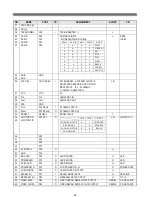
23
29
30
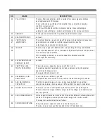
R -Y O U TPU T
B-Y O U TPU T
The m axim um output im pedance of pins 29,and 30 is 500
w hen
PAL/N TSC signals are identified. W hen SEC AM is identified by the
SEC AM add-on and no PAL/N TSC is already identified by the ASM ,
then the ASM sets the -(R -Y)/-(B-Y ) output sw itch open (via D EM SW ).
This enables the -(R -Y)/-(B-Y) outputs of the TD A8395 to be directly
connected to pins 29 and 30 respectively.
31
32
B-Y IN PU T
R -Y IN PU T
The -(B-Y), -(R -Y) output signals (supplied from baseband delay line) are
AC coupled, via a coupling capacitor of 10nF or greater, to the -(B-Y)/
- (R -Y) inputs; both inputs are clam ped during burstkey period.
33
SEC AM R EF O U TPU T
The SEC AM reference output is directly connected to pin 1 of the TD A8395 for
SEC AM decoding;it also can be used as a reference for com b. filter application.
34
35
X-TAL 3.58
X-TAL 4.43
To ensure correct operation of both:
- colour processing internal circuits,
- sync calibration internal circuits,
it is only allow ed to have 3.6M H z X-tals on pin34: both 4.4M H z, 3.6M H z
X-tals are allow ed on pin 35.
If pin35 is not used:then it is left open in application(also XA, XB=0,1).
36
LO O P FILTER BU R ST
PH ASE D ETEC TO R
O ne of the im portant aspects of the PLL is the loop filter connected to pin 36;
it influences the dynam ic perform ance of the loop.
38
C VBS O U TPU T
The output am plitude is 1Vpp (transfer gain ratio betw een C VBS 1int or
C VBS2ext or C VBS3ext/Y S-VH S and C VBS out is 1).
The m axim um output im pedance is 250ߟ.
39
BLAC K PEAK H O LD
C APAC ITO R
For the correct w orking of the black stretcher an external tim e constant should be
added at the black peak hold capacitor input.
40
H O R O U TPU T
This open collector output is m eant to drive the horizontal output stage.
The output is active low,i.e. the line transistor should conduct during
the low period of the output.
41
SAN D C A STLE O U TPU T
/FLYBAC K IN PU T
Pin 41 is a com bined input/output pin.
The pin provides a three level sandcastle pulse.
Both burstkey pulse and vertical blanking pulse are alw ays available, the line
blanking pulse is only present w hen the external flyback pulse is fed to this pin.
The line flyback pulse, fed to this pin is used for tw o functions
- input signal for the PH I-2 loop
- R G B line blanking.
(w ithout flyback pulse blanking occurs only during the burstkey pulse)
To ensure correct w orking of the delay line and SEC AM add-on,
the output should not be loaded w ith m ore than :
- S andcastle input delay line TD A 4665
- S andcastle input S EC AM add-on TD A 8395
42
PH I-2 FILTER /
The loop filter is a first order filter.
FLASH PR O D EC T
This pin requiresa capacitor(C ) only.
A flash protection becom es active w hen this pin is forced>6V.
The horizontal drive is sw itched-off im m ediately.
O nce the voltage is <6V the horizontal drive is sw itched-on again via the slow start
prodecure.
N O
N A M E
D E S CR IPTIO N
Summary of Contents for MV1421
Page 1: ...SERVICE MANUAL MV1421 1422 4822 34cm 48cm Televideo Effective December 1999 MV4822SERV ...
Page 6: ...4 3 BLOCK DIAGRAM 3 1 Audio Signal Flow ...
Page 7: ...5 3 2 Video Signal Flow ...
Page 8: ...6 3 3 TV and monitor power switching ...
Page 22: ...20 3 Block Diagram ...
Page 53: ......
Page 54: ......
Page 55: ......
Page 117: ...2 Main PCB Assy Circuit Diagram SECTION BEFORE AFTER MAIN TUNER ...
Page 118: ...3 SECTION BEFORE AFTER SUB TUNER ...
Page 125: ...10 Exploded View MV1421 model ...
Page 126: ...11 Exploded View MV1422 model ...
Page 127: ...12 Exploded View MV4822 model ...
Page 128: ...13 Exploded View DVT 20F9 model ...
Page 129: ...14 Exploded View DVT 21F1 model ...
Page 130: ...15 Exploded View DVT 21F2 model ...


