22
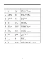
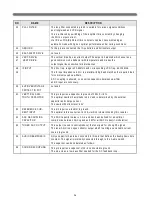
A Voltage detection circuit is connected to both pins.
- pin12 if V12 < 6.8V than a pow er on reset, PO R . is generated.
The H out output is disabled im m ediate.
- pin37 if V37 < 5.8V than the horizontal output is disabled im m ediate.
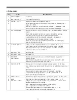
13
17
IN T C VBS IN PU T EXT
C VBS IN PU T
It is recom m ended that the C VBS1 int and C VBS2 ext input am plitudes
are 1Vpp (inclusive sync am plitude).
This, because the noise detector sw itches the
1 loop to slow m ode
(i.e. auto
1 m ode w hen FO A,FO B=0,0) w hen noise level exceeds 100m Vrm s
(i.e. at S/N of 20dB)
14
G R O U N D
All internal circuits are connected to this ground pin 14.
15
AU D IO O U TPU T
The output signal is volum e controlled and is active for both internal and external
audio signals.
The nom inal gain is +12dB and -68dB,w hich gives a total control range of 80dB.
16
D EC O U PLIN G
FILTER TU N IN G
Voltage variations at pin 16, w hich can be due to external leakage current or
crosstalk from interference sources, should be less than 50m V to ensure that tun-
ing of filters/delay cells rem ains correct.
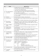
18
BLAC K C U R R EN T
IN PU T
For correct operation of the loop C U R R EN T inform ation is supplied to the black
current input pin.
19
20
21
BLU E O U TPU T
G R EEN O U TPU T
R ED O U TPU T
The R G B output are supplied to the video output stages from pins 21, 20,
and19 respectively.
For nom inal signals (i.e. C VBS/S-VH S,-(R -Y),-(B-Y),TTX inputs) and for nom inal
control settings, then the R G B output signal am plitudes is typically 2V
BLA C K-W H ITE.
22
V-G U AR D IN PU T
/BEAM C U R R EN T
LIM ITER
The beam current lim iting function is realized by reducing the contrast (and finally
the brightness) w hen the beam current reaches too high level.
The circuit falls apart in tw o functions:
- A verage beam current lim iting(AB L):reacting on the average content of the picture
- P eak w hite lim iting (W PL):reacting on high local peaks in the R G B signal.
23
24
25
R ED IN PU T G R EEN
IN PU T BLU E IN PU T
The R IN ,G IN ,BIN signals(nom inal signal am plitude of 700m V)
AC coupled to pin 23,24 and25 respectively.
C lam ping action occurs during burstkey period.
26
R G B IN SE RTIO N
SW ITC H IN PU T
The table below a survey is given of the three m odes w hich can be selected w ith a
voltage on R G B insertion sw itch input pin ;
Vpin26 IIC function Selected R G B signal
0.9V-3V IE1=0 R G B(IN TER N AL)
IE1=1 R in,G in,Bin
(fast insertion on pin 23,24,25)
>4V IE1=X O SD can be inserted at the R G B out pins.
27
LU M IN AN C E IN PU T
An nom inal input signal am plitude of 1V black-w hite M U ST be D C coupled.
50PF;clam ping action occurs during burstkey period.
28
LU M IN AN C E
O U TPU T
The lum inance output signal is approxim ately 1V black-w hite w ith typical
output im pedance of 250 ohm .
N O
N A M E
D E S CR IPTIO N
Summary of Contents for MV1421
Page 1: ...SERVICE MANUAL MV1421 1422 4822 34cm 48cm Televideo Effective December 1999 MV4822SERV ...
Page 6: ...4 3 BLOCK DIAGRAM 3 1 Audio Signal Flow ...
Page 7: ...5 3 2 Video Signal Flow ...
Page 8: ...6 3 3 TV and monitor power switching ...
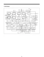
Page 22: ...20 3 Block Diagram ...
Page 53: ......
Page 54: ......
Page 55: ......
Page 117: ...2 Main PCB Assy Circuit Diagram SECTION BEFORE AFTER MAIN TUNER ...
Page 118: ...3 SECTION BEFORE AFTER SUB TUNER ...
Page 125: ...10 Exploded View MV1421 model ...
Page 126: ...11 Exploded View MV1422 model ...
Page 127: ...12 Exploded View MV4822 model ...
Page 128: ...13 Exploded View DVT 20F9 model ...
Page 129: ...14 Exploded View DVT 21F1 model ...
Page 130: ...15 Exploded View DVT 21F2 model ...


