background image

Factory Test & Alignment Specification For MS63F-LA Series (V0.10)

Page 5 of 18

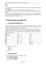
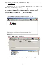
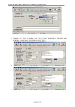
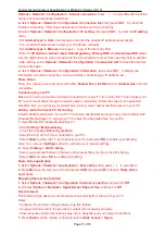
In case of starting from blanked flash, it’s necessary to write first “

V8-6328L01-LB1Rxxx

” file. 

Then, following files need to be written down:

- “

MS6328LA_FULL_UPGRADE.bin

See Appendix

n

How to upgrade FLASH SW using Mstar tool

”   

See Appendix

o

“How to upgrade FLASH SW using USB”

1.3. Project ID Modification   

There are different IDs stored into the NVM depending on different Panels settings and Models 

features, but there’s only one key branching ProjectID that includes all. So, it’s not recommended to 

modify Panel ID with Hyper terminal as other ID features may not change! 

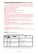
To modify Project ID, you need to go through “

Design menu

Æ

Service menu

Æ

Project ID

”, then 

spin left or right with RCU “

Zoom±

” keys to suitable ID (Project name is dynamically refreshed).

See Appendix

p

How to change Project ID with RCU

”   

Here below is none exhaustive ProjectID table for reference:   

MODEL

ProjectID

Panel Name

L32E5300

001

L46E5300F

002

L42E5300F

003 

L42D4330F3D

004

L39E5300F/CMI

005

L39E5300F/AUO

006

… 


1.4. Functional Test

Once the boards (chassis, KB, IR, PSU…) and the panel are well interconnected, plug all 

external generator devices to relevant inputs/outputs below according to their respective test patterns 

format and check picture content and sound quality accordingly: 

Source

Test Signal

Test Pattern

Analog /Digital Tuner

(VHF/UHF & CATV) 

RF cable generator

2D - Movie 1280x720

2D - Static Picture 1920x1080 

1.

Frequency Range: full band

2.

Standard: NTSC /PAL M

3.

ISDB-T 

SPDIF

(optical)

Audio Amplifier

PCM or Dolby D+ 

AV1 IN


(CVBS & AUDIO) 

Chroma/Fluke

generator

PAL Half Color & Gray bars

AV2 IN


(CVBS &AUDIO) 

Chroma/Fluke 

generator

PAL Half Color & Gray bars 720x576

Half Color & Gray bars

VGA  

Chroma/QuantumData

UXGA - 1600x1200@60Hz

Summary of Contents for MS63F-LA

Page 1: ... LIGNMENT 0ROCEDURE ˊ LOCK DIAGRAM ˊ3CHEME IAGRAM 4ROUBLESHOOTING om list 4HIS M ANUAL I S T HE L ATEST AT T HE T IME OF PR INTING AND DOE S NOT INCLUDE THE MODIFICATION WHICH MAY BE MADE AFTER THE PRINTING BY THE CONSTANT IMPROVEMENT OF PRODUCT ...

Page 2: ...lectric shock to the person The exclamation point within an equilateral triangle is intended to alert the user to the presence of important operating and maintenance servicing instructions in the literature accompanying the appliance CAUTION Use of controls adjustments or procedures other than those specified herein may result in hazardous radiation exposure CA U T ION RISK RISK OF ELECTRI ELECTRI...

Page 3: ...o impact of any kind Be particularly careful not to damage the picture tube surface 9 Unplug this television set from the wall outlet before cleaning Do not use liquid cleaners or aerosol cleaners Use a damp cloth for cleaning 10 1 Do not place this television set on an unstable cart stand or table The television set may fall causing serious injury to a child or an adult and serious damage to the ...

Page 4: ...ing conductors location of antenna discharge unit connection to grounding electrode and requirements for the grounding electrode 15 2 Note to CATV system installer Only for the television set with CATV reception This reminder is provided to call the CATV system attention to Article 820 40 of the NEC that provides guidelines for proper grounding and in particular specifies that the cable ground sha...

Page 5: ...edurein youroperatinginstructions do not attempt any further adjustment Unplug the set and call your dealer or service technician 22 Whenever the television set is damaged or fails or a distinct change in performance indicates a need for service unplug the set and have it checked by a professional service technician 23 It is normal for some TV sets to make occasional snapping or popping sounds par...

Page 6: ...rs Bottom side AV System PAL NTSC Audio Power Output 8W 2 TV Channels Analog Cable 1 125 Antenna 2 69 Sound Processing BTSC SAP Stereo Mono TV Channels Digital Antenna 7 69 Dolby Virtual Surround MS10 DD DP Chassis MS63F LA AVC Auto Volume Control Yes Certification CB SRS Yes Power Supply AC 100V 240V 50 60Hz Sound Features MTS AVC Equalizer Surround Power Consumption TV on 90W Sound Control Volum...

Page 7: ...nt Specification For MS63F LA Series V0 10 Page 1 of 18 TCL World Wide R D FPD CENTER Factory Test Alignment Specification FTAS for MS63F LA Series Version 0 10 PREPARED BY Jianwei Li DATE 2012 09 12 APPROVED BY _____ DATE ...

Page 8: ...oprietary to TCL SZ FPD lab and shall not be disclosed by the recipient to third persons without the written permission of the team leader or GM of R D Revision History Version Issue Date Description of changes v0 10 2012 8 12 This is the draft version of normal SIACP HDMI as the main absolute input The password of factory menu is 9735 ...

Page 9: ...S audio 1 Side AV CVBS audio 1 AV OUT 1 USB thumb drive 2 Picture Video Audio Playback Hub Mouse Keyboard rd Headphone output 1 SPDIF output Optical Functions OAD WIFI Ready USB Dongle accessory IEEE 802 11 b g n DIVX DLNA DMP Internet Opera 3D auto top bottom side by side frame sequencing 1920x2205 24Hz 1920x1080p x2 1280x1470 50Hz 1280x720p x2 1280x1470 60Hz 1280x720p x2 Passive Glasses Audio Re...

Page 10: ... Check Before power on please check the board according to the relevant block diagram and circuit diagram and make sure that no serious issue or mistake can destroy the board For example the output of DC DC and LDO should not be shorted to ground Supply a suited voltage and power on then check the voltage according to the relevant block diagram circuit diagram and voltage spec the error should les...

Page 11: ...D Project name is dynamically refreshed See Appendix p How to change Project ID with RCU Here below is none exhaustive ProjectID table for reference MODEL ProjectID Panel Name L32E5300 001 L46E5300F 002 L42E5300F 003 L42D4330F3D 004 L39E5300F CMI 005 L39E5300F AUO 006 1 4 Functional Test Once the boards chassis KB IR PSU and the panel are well interconnected plug all external generator devices to ...

Page 12: ...ot any ADC to perform 1 6 DDC EDID T Link Test The E EDID data structures are according to VESA Enhanced EDID 1 3 and EIA CEA 861B for HDMI CEA Timing Extension structure has been extended to support all 3D capable timings All VGA and HDMI structures have their own BIN profile which are part of main SW and uploaded at power on into HDMI switch chipset For EDID check it s needed to check whether th...

Page 13: ...SW will internally manage Network ID NID flag controlling all MAC DID UID integrity to facilitate PA screening further Note It s not necessary to check video and audio from DLNA server See Appendix v v NETWORK CONNECTION AND TEST 2 Product Assembly PA Test Alignment 2 1 Factory Menu Follow the below steps to pop up the Factory menu in case of FactoryKey is disabled Press RCU MENU key to display ma...

Page 14: ...n be considered as Burn In Additional Aging for White Balance alignment is no more necessary due to consistent Picture Performance with Cloning usage This function is accessible by selecting Factory menu ÆWARM UP pressing RCU Zoom key and then leaving Factory menu Other faster methods are available on above enclosed SIACP requirements rev v3 9 2 3 White Balance WB White Balance Touch Up As some co...

Page 15: ...uned Targets and Tolerances for all inputs The measured parameters should be mainly x y coordinates The Y peak luminance measurement at 100IRE is depending on achievable panel performance and less important than saturation on high light If necessary Scaling Contrast register can be adjusted The BlackLevel measurement need to be within 1 2 If necessary Scaling Brightness register can be adjusted Th...

Page 16: ... default presets This function is accessible by selecting Factory menu ÆSHOP init then pressing RCU OK key Other faster methods are available on above enclosed SIACP requirements rev v3 9 Appendix n How to upgrade SW FLASH using Mstar tool Open Mstar Mboot software programming tool ISP_Tool_4528 Click on Read and select mboot bin file Then click Connect it will check SPI FLASH s tape correct it wi...

Page 17: ...Factory Test Alignment Specification For MS63F LA Series V0 10 Page 11 of 18 Next click on Auto menu then click Run it begin programming Mboot bin when programming success it will display a word Pass ...

Page 18: ...then press RCU OK key Switch off TV by removing AC cord Reconnect AC cord to restart TV and wait few seconds for Eeprom update The second method To use this method there should be SW in mainboard to ensure TV can display normally Copy the SW BIN image V8 6328L01 LF1RXXX bin into USB stick pen drive root path Press RCU MENUÆSettingÆFunctionÆsoftware upgradeÆOKÆBy USB TV display a warning informatio...

Page 19: ...Normal one Normal is the default Tone mode R Gain 000 255 R White balance 127 128 for gain G Gain 000 255 G White balance 127 128 for gain B Gain 000 255 B White balance 127 128 for gain R Offset 000 255 R Gray balance 127 128 for offset G Offset 000 255 G Gray balance 127 128 for offset B Offset 000 255 B Gray balance 127 128 for offset White Balance Init DO Press OK key to initial the preset RGB...

Page 20: ...on after switching on power STB Force TV to start in standby Last Force TV to start from last power status 9 USB UPDATE submenu Item Sub item Value Note USB UPDATE Main Upgrade Upgrade software MEMC Upgrade Upgrade MEMC HDCP Uprade Upgrade HDCP Mboot upgrade Upgrade Mboot NVM Upgrade Upgrade NVM NVM backup Backup NVM CH list Upgrade Upgrade CH list CH list backup Backup CH list 0 DeviceID test sub...

Page 21: ...d DID to the factory local service and the service connect to the factory LAN When product line produce the IPTV there will be a work station PC normally down load the DID UID and also MAC from the local service then using UART command sent them to the module 2 How to test the function When there is a module need to test the Device function connect the set to the LAN use the device ID test the mod...

Page 22: ...2 3 Connection Methods You can setup the wireless network connection three ways 1 2 3 1 Scan Select Wireless setting Scan then press OK the TV will scan all access points within range The access points found by the TV will be displayed Select an available access point then press OK to connect the TV to it Notes If you select a protected access point you will have to enter the corresponding passwor...

Page 23: ...twork cable or wirelessly Follow the steps in turn specified hereafter then you can enjoy recorded video picture music and or text files saved on your PC Adding media from your PC for sharing Install a DLNA media server in your PC The simple and familiar server you may install is Microsoft Windows Media Player 11 Allow your TV to share the designated files on your PC 1 Open Microsoft Windows Media...

Page 24: ...Repeat this step until you have created as many folders as you d like Visit a bookmark Go to a bookmark by simply clicking its name instead of having to type its address Delete a bookmark Click the Delete icon after a link to delete the link if you want to Edit a bookmark Click the Edit icon after a link to edit the name and or URL of the bookmark if you want to Click Close bookmark manager bar to...

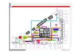
Page 25: ...R L Amplifier POWER IR KEY LVDS MS6328 DDR LVDS USB Flash Audio VGA YPbPr CVBS IF TMDS IR IPTV DDR1 DDR2 DEMO TS TS8121 FLASH ...

Page 26: ...ED TO UNAUTHORIZED PERSONS COPIEDUNLESS PERMITTED IN WRITING FORMAT DIN A4 SBU ON BY OF PAGE Last saved DESIGNATION TCLNO TCL PAGE2 TUNER MSD6328BX TCL DESIGN PAGE3 POWER SUPPLY INTERFACE PAGE1 INDEX PAGE4 MSD6328 PAGE5 DDR PAGE6 YPBPR AV IN VGA IN PAGE7 HDMI SWITCH PAGE8 USB LVDS PAGE9 AMPLIFIER PAGE10 ISDB 1 25 MT5311B 18 SEP INITIAL VERSION 18 SEP SHENZHEN V0 1 INDEX 7 16 2012_14 17 ...

Page 27: ...ND CABLE AIR TU_3V3 IF_AGC NC 0R R100 3V3 R115 10R R117 NC 0R R175 10K R171 10K R198 NC 0R IF AGC SEL R174 100K R109 56R R105 33R R116 NC 0R R176 10K D_IF2 D_IF1 D_IF_AGC R173 100K B E C Q133 BT3906 B C E Q134 BT3904 B C E Q132 BT3904 B E C Q131 BT3906 R172 100K TU_3V3 R107 56R R104 33R 120P C153 T_SCL 12 11 10 9 8 7 6 5 4 3 1 2 U103 PE42750 R126 4K7 X16M1 16M 100NH L106 L105 8 2NH 2 4NH L104 TU_3...

Page 28: ... 15 11 10 6 16 2 3 12 9 14 7 5 U203 TPS54418 C262 0 1U C261 10U 5V 1 2 3 4 U209 LD1117S33 C272 0 1U 10U C271 10U C216 C251 0 1U DTMB 1V2 DEMO_1V2 R262 NC 0R 5V 1 2 3 4 U200 LD1117S33 4 1 2 3 U208 AS1117AD VCC_VSENSE 1V2 R261 1R2 33K NC R251 R257 47K NC 5V 5 6 3 2 1 4 U202 MP2127 R24 0R NC R25 0R NC 10U C214 10U C204 C289 2U2 3V3 10U C212 C213 100U 16V 10U C260 C200 220U 16V R222 NC 0R 2 3 1 U200A ...

Page 29: ...MSTIC 3DSELECT PCM_A4 UART TX2 SPI_SCK BIN2 GIN2 GIN2N RIN2 YPBPR_PB TS_MDO0 OSDA0 VGA_L_IN AC9 AD8 AD9 AE7 AE8 AC8 AE10 AC10 AD10 AB5 AB7 AA8 AB8 Y10 AB6 AA6 Y9 AB10 AA7 AA9 AA4 AA5 AA2 AA1 AB2 AB1 AA3 Y2 W3 AA16 AC16 Y17 AC15 AC13 AD13 AD14 AC14 AA15 AB16 Y16 Y13 Y15 AD15 AC17 AC18 AB13 Y12 AA13 AB11 AE17 AD16 AD17 AA17 AC12 AA12 AE13 AE14 AE16 Y14 AD18 AA14 AB14 AE11 AC11 AA11 AD12 AA10 AD11 Y1...

Page 30: ...K7 K9 T2 J7 U401 K4B2G1646C A_DDR3_WEZ A DDR3 WEZ A DDR3 A0 A_DDR3_A0 1 2 3 4 5 6 7 8 R423 22R 1V5 R18 10K R19 10K 1V5 1V5 R16 10K R17 10K C11 B13 A10 C9 C15 A8 C14 C10 A13 B10 B15 C13 A14 B9 B12 A11 B11 C12 B7 A7 B14 C8 B8 C16 B22 C17 A22 B18 A23 B17 C22 A17 D17 E20 E17 C20 F18 B20 F17 D20 C18 B21 A16 B16 C19 A19 D18 E18 F23 H25 E24 C24 J23 D24 H23 C23 H24 E25 K24 G23 J24 D23 G24 F24 G25 E23 A24 ...

Page 31: ...03 SIDEAV AV 1 2 3 4 5 6 P505 GND13 C532 0 1U R556 10K R546 100R C540 47P C539 47P C538 47P C528 47P 75R R549 R507 12K R505 12K R506 10K R504 10K R526 12K R522 75R R523 75R R524 75R R528 12K R525 10K R527 10K 75R R547 75R R548 R516 100R R529 100R R560 10K R561 100R R531 100R R519 100R R541 220R R503 75R R543 220R R542 47K R540 470R R544 47K R545 1K R500 470R R538 6K8 R532 22K R534 10K R535 10K R53...

Page 32: ... 16 17 18 19 P600 HDMI3 HPD HDMI3 RX2N HDMI3_5V HDMI3 DDC SDA HDMI3 CLKP HDMI3 DDC SCL HDMI_ARC CEC HDMI3 CLKN HDMI3 RX0N HDMI3 RX0P HDMI3 RX1N HDMI3 RX1P HDMI3 RX2P HDMI2 HPD HDMI2_5V HDMI2 DDC SDA HDMI2 DDC SCL CEC HDMI2 CLKN HDMI2 CLKP HDMI2 RX0N HDMI2 RX0P HDMI2 RX1N HDMI2 RX1P HDMI2 RX2N HDMI2 RX2P HDMI1 HPD HDMI1_5V CEC HDMI1 DDC SCL HDMI1 DDC SDA HDMI1 CLKN HDMI1 CLKP HDMI1 RX1N HDMI1 RX0N ...

Page 33: ...T3904 C761 0 1U NC 4K7 R764 R763 5K6 R762 22K 4K7 R761 0R R734 3DSELECT R752 0R R751 NC 0R 1 2 3 4 5 6 7 8 9 10 11 12 13 14 15 16 U700 TS8121CLF R703 100R CFG PWM0 2V5 R724 0R R717 3K3 R719 2K7 R716 4K7 R704 100R R706 100R R709 100R R705 100R R708 100R 1 2 4 6 8 12 14 16 18 20 10 22 24 26 28 3 5 7 9 11 13 15 17 19 21 23 25 27 29 30 32 34 36 38 40 31 33 35 37 39 P702 PANEL_VCC 3D_EN P_VCC 3D_FLAG B...

Page 34: ...45 44 43 42 41 40 39 38 37 35 34 33 32 31 30 29 28 27 26 25 24 23 22 21 20 19 18 17 16 15 14 13 11 10 9 8 7 6 5 4 3 2 1 36 12 48 U800 STA381BW HP_R HP_L C802 0 22U C803 0 22U L808 33UH L807 33UH L806 33UH L809 33UH SPK_R SPK_R SPK_L SPK_L ASDATA0 C800 1U C821 0 1U C840 330P R804 22R R811 10K R812 10K 5 4 1 2 3 P800 33R R826 R825 33R 33R R824 R823 33R R809 27K 27K R808 R813 100R R814 100R 600R L810...

Page 35: ... 39 38 37 35 34 33 32 31 30 29 28 27 26 25 24 23 22 21 20 19 18 17 16 15 14 13 11 10 9 8 7 6 5 4 3 2 1 36 12 U905 TC90527FG 100P C938 R935 33R 0 1U C932 0 1U C931 NC 0 1U C930 L901 NC 1 8UH R932 0R R931 0R 0 1U C923 C922 1U 0 1U C921 C920 1U 0 1U C918 0 1U C917 0 1U C916 0 1U C915 C914 1U 0 1U C912 0 1U C910 0 1U C909 C908 NC 18P NC 18P C907 C906 0 1U C905 10P C904 10P 0 1U C903 0 1U C902 C901 1U ...

Page 36: ... IIC bus Check the peripheral circuit of mail IC check solder of main IC check data fo NVM and reset it Check reset signal of main no switch on Check 3 3V 12V 24V of power supply Check PW Check DC DC part check Check signal P ONˈ DIMBL ON of main IC link to PW Trouble shooting ...

Page 37: ...n IC check LVDS cable Check crystal frequence Check the peripheral circuit of mail IC updating SW reset NVM replace main IC Abnormal picture All signal source bad Individual signal source bad Check the path with this signal source Check panel ID ...

Page 38: ...te function Abnormal sound Check all sound source Individual sound signal source Check the sound signal link to main IC Check the peripheral circuit of main IC SW Check the power of sound IC Check sound IC Check wave filter and speaker Y ...

Reviews: