


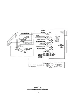


4.2 COMPONENTS OF THE
DRIVE
The drive contains the electrical and mechanical
components required to perform four major
functions:
1. Generate and interpret control signals.
2. Position the read/write head(s) to the
desired track.
3. Write and read data.
4. Control the spindle.
The electrical and mechanical components of
the drive are connected together via four- and
five-pin connectors. This allows the individual
assemblies to be removed (Figure 4-4).
4.3 GENERATE AND
INTERPRET CONTROL
SIGNALS
The components of the drive required to gener
ate and interpret the control signals are:
1. Index Sensor
2. Write Protect Switch
3. Track 0 Switch
4. Drive Select
INDEX SENSOR
The Index signal is derived from an infrared
L.E.D. and phototransistor detector. When the
index/sector hole in the diskette passes through
the index sensor, the light from the L.E.D. is al
lowed to turn on the index detector, producing a
positive pulse on J4, Pin 15 (Figure 4-5).
This signal is shaped by an input buffer, Q8, and
supplied to inverter IC 2E. Then, it is gated with
Drive Select for an output control signal at the
interface Jl, Pin 8.
WRITE PROTECT SWITCH
The Write Protect signal is derived from a me
chanical switch integrated into the drive, the
switch is deactivated, causing a high signal on
J4, Pin 5. Then, it is buffered and inverted to dis
able the Write Enable signal. It is also gated
with drive select, producing an output signal on
the interface.
TRACK 0 SWITCH
The Track 0 sensor signal is derived from a me
chanical switch internal to the drive. As the
head carriage moves back toward Track 0, the
switch is activated between Tracks 0 and 3.
This low active signal comes in via Connector
Pll, Pin 1, and is supplied to a latch that
debounces the switch noise (Figure 4-6). The
combination of the Track 0 switch being activat
ed and the proper stepper motor phase (Phase 0)
produces all high signals at IC 4B, pins 9,10,12,
and 13, causing a low output at IC 4B, Pin 8
(Test Point 8). Then, this signal is buffered
through IC 3D, Pins 1 and 2, which inhibits step
ping to Track 0 minus 1. IC IF Pins 11, 12, and
13 gate the Track 0 output with Drive Select, to
give a Track 0 output to Pin 26 of the interface.
DRIVE SELECT
The Drive Select signal is derived from the host
controller through the interface connector.
R14 holds the output of the appropriate select
line high until the line is driven low. This signal
is buffered through IC 3E and IC 3D, which en
ables the drive electronics.
The front panel L.E.D. is driven by the select
logic through IC 3E, Pins 3 to 4. If the drive is
not selected through the select jumpers, and the
MX jumper is not cut, the drive electronics are
active but the front panel L.E.D. is not on.
4-3
Summary of Contents for TM100-1
Page 8: ......
Page 11: ...FIGURE 1 1 DISK DRIVE ...
Page 12: ......
Page 18: ......
Page 29: ...WRITE PROTECT TAB WRITE PROTECT TAB FIGURE 3 5 WRITE PROTECT TAB ...
Page 34: ...FIGURE 4 4 INTERCONNECT BLOCK DIAGRAM 4 4 ...
Page 58: ...CARRIAGE ASSEMBLY FIGURE 5 14 UPPER ARM AND SCREWS ...
Page 66: ...FIGURE 6 2 LOGIC CIRCUIT BOARD MOUNTING 6 8 ...
Page 72: ...E RIN G C O N E SH A FT FIGURE 6 7 CONE S COMPONENT PARTS 6 14 ...
Page 76: ...FIGURE 6 13 INDEX EMITTER SENSOR S MOUNTING AND CABLE HARNESSING 6 18 ...
Page 79: ...FIGURE 6 16 DRIVE MOTOR HARNESSING AND MOUNTING 6 21 ...
Page 82: ...FIGURE 6 19 TRACK 0 ADJUSTMENT SCREW 6 24 ...
Page 86: ...FIGURE 6 24 UPPER ARM SCREWS 6 28 ...
Page 87: ...MOUNTING FIGURE 6 26 FELT PAD ON UPPER ARM 6 29 ...
Page 90: ......
Page 92: ...A 2 ...
Page 93: ...A 3 ...
Page 94: ......
Page 99: ...l a n d e i n CORPORATION LOGIC CIRCUIT BOARD SCHEMATIC 180011 REV F SHEET 2 OF 3 B 5 ...
Page 100: ... SV SHEET 3 OF 3 B 6 ...