5.3 RF Trace Layout Design
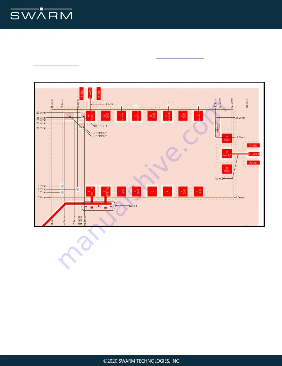
The Tile is certified with a PCB edge SMA connectors
[
for the RF and GPS outputs, with a micro-strip trace layout (along with
copper keep-out areas) as shown in
Figure 8
.
Figure 8:
RF trace routing and keep out area for RF output (top layer).
Note 1:
The location for the module input and bypass capacitance.
Note 2:
SAT_RF track should utilize a 50 Ohm micro-strip specific to the customer board layout,
with a ground plane below.
Note 3:
GPS_RF track should utlize a 50 Ohm micro-strip specific to the customer board layout,
with a ground plane below.
Note 4:
Mounting holes - 1.067mm diameter. Not required in customer design
October 2020
Swarm Tile Manual - Rev 1.10
30/65


