background image

2-24

Supermicro C7X99-OCE/C7X99-OCE-F Motherboard User’s Manual

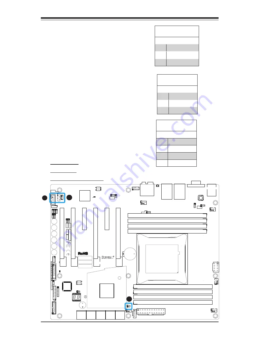
DOM PWR Connector (JSD1)

The Disk-On-Module (DOM) power con-

nector,  located  at  JSD1,  provides  5V 
(Gen1/Gen) power to a solid state DOM 

storage device connected to one of the 
SATA ports. See the table on the right 

for pin definitions.

DOM PWR

Pin Definitions 

Pin#     Definition     

1

5V

2

Ground

3

Ground

MAC CODE

IPMI CODE

BAR CODE

C7X99-OCE-F

SW_BIOSRC

S4

S7

S10

S5

S6

S9

OC_FR

ONT_P

ANEL

S8

S11

CLR_CMOS_SW

JUSB30_I2

JA

UDIO1

LED4

I-SATA0

I-SATA2

I-SATA4

S-SATA0

S-SATA2

AUDIO_FP

JIPMB1

JSD1

MH11

MH2

MH9

MH10

JPW2

C

A

LEDM1

JBT1

BT1

+

FAN5

FAN4

FAN1

1

FAN2

4

FAN3

JPL2

JPUSB1

J29

J30

JP

ME2

JPAC1

JPL1

JI2C1 JI2C2

JPB1

JPG1

JWD1

1

JL2

JL1

JD1

1

JF1

2

19

JPI2C1

JSTBY1

JTP
M1

SP1

+

HD AUDIO

VGA

LAN1

LAN2

USB 16/17(3.0)

USB 12/13(3.0)

USB 10/11(3.0)

USB 14/15(3.0)

CPU SL

O

T6 PCI-E 3.0 X16

PCH SL

O

T5 PCI-E 2.0 X1  (IN X4)

CPU SL

O

T4 PCI-E 3.0 X8 (IN X16)

PCH SL

O

T3 PCI-E 2.0 X1  (IN X4)

CPU SL

O

T2 PCI-E 3.0 X8 (IN X16)

CPU SL

O

T1 PCI-E 3.0 X8 (IN X16)

2-3:DISABLE 1-2:ENABLE

:W

AT

CH DOG

SPEAKER PWR LED

:TP

M/POR

T80

CPU

CHASSIS INTRUSION

JI2C2

2-3:DISABLE 1-2:ENABLE JI2C1

PWR ON

OH/FF

NIC1

NIC2

RST

X

CMOS CLEAR

1-2:NORMAL

2-3:BIOS RECOVERY

JBR1

PWR LED

HDD LED

NMI

X

2-3:ME M

ANUF

AC

TURING MODE

JP

ME2

1-2:NORM

AL

1-2 ENABLE

2-3 DISABLE

1-2 ENABLE

2-3 DISABLE

:PWR I2C

1-2 ENABLE

2-3 DISABLE

2-3 DISABLE 1-2 ENABLE

1-2 ENABLE

2-3 DISABLE

JPAC1

VGA

USB14/15 WAKE UP

1-2 RST

2-3 NMI

:SATA DOM POWER

DIMMD2

DIMMD1

DIMMC2

DIMMC1

DIMMB2

DIMMB1

DIMMA2

DIMMA1

JBR1

JWD1

JPW1

JPUSB1

JPB1

JPG1

C

A

LED1

I-SATA1

I-SATA3

I-SATA5

S-SATA1

S-SATA3

C7X99-OCE/

COM1

A

B

A. DOM Power

B STBY PWR 

C System Management Bus

Standby Power Header (STBY1)

The Standby Power header is located 

at  STBY1  on  the  motherboard.  See  the 
table on the right for pin definitions.

Standby Power

Pin Definitions

Pin#     Definition     

1

+5V Standby

2

Ground

3

Wake-up

System Management Bus (JIPMB1

)

A System Management Bus header for the 
IPMI slot is located at IPMB. Connect the 
appropriate cable here to use the IPMB 

I2C  connection  on  your  system.  For  the 

C7X99-OCE-F only.

System Management 

Bus

Pin#     Definition     

1

Clock

2

Ground

3

Data

4

No Connection

C

Summary of Contents for Supero C7X99-OCE

Page 1: ...C7X99 OCE C7X99 OCE F USER S MANUAL Revision 1 0...

Page 2: ...mits for a class B digital device pursuant to Part 15 of the FCC Rules These limits are designed to provide reasonable protection against harmful interference in a residential installation This equipm...

Page 3: ...chap ter when installing the processor memory modules and other hardware components into the system If you encounter any problems see Chapter 3 which describes trouble shooting procedures for video me...

Page 4: ...ro C7X99 OCE C7X99 OCE F Motherboard User s Manual Checklist Congratulations on purchasing your computer motherboard from an ac knowledged leader in the industry Supermicro boards are designed with th...

Page 5: ...ng Warnung Bei Einsetzen einer falschen Batterie besteht Explosionsgefahr Ersetzen Sie die Batterie nur durch den gleichen oder vom Hersteller empfohlenen Batterietyp Entsorgen Sie die benutzten Batte...

Page 6: ...ante Supermicro C7X99 OCE C7X99 OCE F Motherboard User s Manual Waarschuwing Er is ontploffingsgevaar indien de batterij verkeerd vervangen wordt Ver vang de batterij slechts met hetzelfde of een equi...

Page 7: ...roducto debe seguir todas las leyes y reglamentos nacionales Attention La mise au rebut ou le recyclage de ce produit sont g n ralement soumis des lois et ou directives de respect de l environnement R...

Page 8: ...ro com Europe Address Super Micro Computer B V Het Sterrenbeeld 28 5215 ML s Hertogenbosch The Netherlands Tel 31 0 73 6400390 Fax 31 0 73 6416525 Email sales supermicro nl General Information support...

Page 9: ...the links below to download all necessary drivers utilities and the user s manual for your motherboard SMCI product manuals http www supermicro com support manuals Product Drivers and utilities ftp f...

Page 10: ...pecial Features 1 4 Recovery from AC Power Loss 1 4 1 5 PC Health Monitoring 1 4 Fan Status Monitor with Firmware Control 1 4 Environmental Temperature Control 1 4 System Resource Alert 1 5 1 6 ACPI F...

Page 11: ...2 16 PS 2 Keyboard Mouse Port 2 17 VGA Port C7X99 OCE F only 2 17 Front Control Panel 2 18 Front Control Panel Pin Definitions 2 19 Power LED 2 19 HDD LED 2 19 NIC1 NIC2 LAN1 LAN2 2 19 Overheat OH Fa...

Page 12: ...store S11 2 33 2 9 Onboard Indicators 2 34 LAN 1 LAN 2 LEDs 2 34 BMC Heartbeat LEDM1 2 34 Power LED LED1 2 35 Status Display LED4 2 35 2 10 SATA Connections 2 36 SATA Connections I SATA0 I SATA9 2 36...

Page 13: ...rt the Setup Utility 4 2 4 2 Setup Home 4 3 Load Optimized Defaults 4 5 Save All Settings Only 4 5 Save Settings to OC3 4 5 Exit Without Save 4 5 Save and Reset 4 5 Save and Exit Setup 4 5 4 3 System...

Page 14: ...16 6 Core Ratio Limit 4 16 7 Core Ratio Limit 4 16 8 Core Ratio Limit 4 16 CPU Cache Ratio 4 16 BCLK Ratio 4 17 BCLK Clock Frequency 1 100 MHz 4 17 Internal PLL Overvoltage 4 17 CPU BCLK Filter PLL Fr...

Page 15: ...ge Target mV 4 20 FIVR Faults Enable 4 20 FIVR Efficiency Enable 4 20 CPU Overclocking 4 20 CPU Input Voltage 4 20 Memory Overclocking 4 21 Load Memory Profiles 4 21 Memory Timing Configuration Expert...

Page 16: ...PCI E 3 0 X16 OPROM 4 37 Onboard LAN Option ROM Type 4 37 Onboard LAN1 Option ROM Onboard LAN2 Option ROM 4 37 Onboard Video Option ROM C7X99 OCE F Only 4 37 VGA Priority 4 37 USB Settings 4 38 Legacy...

Page 17: ...ot Mode 4 46 Key Management 4 46 Default Key Provision 4 46 Enroll All Factory Default Keys 4 46 Save All Secure Boot Variables 4 46 Platform Key 4 46 Delete PK 4 46 Set New PK 4 47 Key Exchange Key 4...

Page 18: ...cision Event Timer 4 50 Console Redirection Settings 4 51 COM 1 4 51 Enable Console Redirection 4 51 SOL 4 53 4 11 IPMI 4 57 IPMI 4 57 System Event Log 4 57 SEL Components 4 57 Erasing Settings 4 58 E...

Page 19: ...ix C UEFI BIOS Recovery Instructions C 1 An Overview to the UEFI BIOS C 1 C 2 How to Recover the UEFI BIOS Image the Main BIOS Block C 1 C 3 To Recover the Main BIOS Block Using a USB Attached Device...

Page 20: ...xx Notes Supermicro C7X99 OCE C7X99 OCE F Motherboard User s Manual...

Page 21: ...bility for overclocking platforms in a sleek package Please refer to our website http www supermicro com products for proces sor and memory support updates 1 2 Chipset Overview Intel X99 Express Chips...

Page 22: ...anes compared to 40 with other CPU models Two 2 PCI Express 2 0 x1 in x4 slots Network Connections Two 2 Gigabit Ethernet Controllers Intel i210 AT gigabit LAN controller IPMI support shared with LAN1...

Page 23: ...overy Health Monitoring CPU Monitoring Onboard voltage monitors for 1 05V 5V 12V VBAT Memory CPU Core CPU 8 phase switching voltage regulator CPU System overheat LED and control CPU Thermal Trip suppo...

Page 24: ...becomes unstable a warning is given or an error mes sage is sent to the screen The user can adjust the voltage thresholds to define the sensitivity of the voltage monitor Fan Status Monitor with Firmw...

Page 25: ...ng its hardware operating system and application software This enables the system to automatically turn on and off peripherals such as CD ROMs network cards hard disk drives and printers In addition t...

Page 26: ...wer supply that meets ATX power supply Specification 2 02 or above It must also be SSI compliant For more information please refer to the web site at http www ssiforum org Additionally in areas where...

Page 27: ...therboard Image Note All graphics shown in this manual were based upon the latest PCB Revision available at the time of publishing of the manual The motherboard you ve received may or may not look exa...

Page 28: ...4 1 1 19 Important Notes to the User See Chapter 2 for detailed information on jumpers I O ports and JF1 front panel connections indicates the location of Pin 1 Jumpers not indicated are for testing...

Page 29: ...RST X CMOS CLEAR 1 2 NORMAL 2 3 BIOS RECOVERY JBR1 PWR LED HDD LED NMI X 2 3 ME MANUFACTURING MODE JPME2 1 2 NORMAL 1 2 ENABLE 2 3 DISABLE 1 2 ENABLE 2 3 DISABLE PWR I2C 1 2 ENABLE 2 3 DISABLE 2 3 DI...

Page 30: ...ernal Speaker Pins 3 4 Buzzer JF1 Front Panel Control Header JL1 Chassis Intrusion Header JPW1 24 pin ATX Main Power Connector Required JPW2 12V 4 pin CPU power Connector Required JSD1 SATA DOM Disk O...

Page 31: ...er 2 Installation 2 1 Installation Components and Tools Needed Screws Phillips Head Screwdriver Processor DDR4 DIMMs PC Chassis Heatsink with Fan Power Supply Video Card Optional SATA USB Optical Driv...

Page 32: ...its edges only do not touch its components peripheral chips memory modules or gold contacts When handling chips or modules avoid touching their pins Put the motherboard and peripherals back into thei...

Page 33: ...atsink If you buy a CPU separately make sure that you use an Intel certified multi directional heatsink only Make sure to install the system board into the chassis before you install the CPU heatsink...

Page 34: ...down on the Open 1st lever to open the load plate Lift the load plate to open it completely OPEN1st WARNING OPEN1st WARNING 2 Press down on Load Lever Close 1st WARNING Pull lever away from the socke...

Page 35: ...nce they are aligned carefully lower the CPU straight down into the socket Do not drop the CPU on the socket Do not move the CPU horizontally or vertically Do not rub the CPU against the sur face or a...

Page 36: ...r Lock Push down and lock Open 1st lever Push down and lock Close 1st lever Gently close the load plate 1 2 3 4 7 Close the load plate with the CPU inside the socket Lock the Close 1st lever first the...

Page 37: ...Place the heatsink on top of the CPU so that the two mount ing holes on the heatsink are aligned with those on the retention mechanism Note Graphic drawings included in this manual are for reference o...

Page 38: ...ed to remove the heatsink please follow the instruc tions below to uninstall the heatsink to avoid damaging the CPU or other components 1 Unplug the power cord from the power supply 2 Loosen the screw...

Page 39: ...3 NMI SATA DOM POWER DIMMD2 DIMMD1 DIMMC2 DIMMC1 DIMMB2 DIMMB1 DIMMA2 DIMMA1 JBR1 JWD1 JPW1 JPUSB1 JPB1 JPG1 C A LED1 I SATA1 I SATA3 I SATA5 S SATA1 S SATA3 C7X99 OCE COM1 2 4 Installing DDR4 Memory...

Page 40: ...B 4GB 4GB 4GB 4GB 4GB 32GB 8GB 8GB 16GB 8GB 8GB 8GB 8GB 32GB 8GB 8GB 8GB 8GB 8GB 8GB 48GB 8GB 8GB 8GB 8GB 8GB 8GB 8GB 8GB 64GB The C7X99 OCE F supports up to 64GB of Unbuffered UDIMM DDR4 non ECC 2133...

Page 41: ...Win dows Vista This change is specific to the behavior of Physical Address Extension PAE mode which improves driver compat ibility For more information please read the following article at Microsoft s...

Page 42: ...ABLE 2 3 DISABLE 1 2 ENABLE 1 2 ENABLE 2 3 DISABLE JPAC1 VGA USB14 15 WAKE UP 1 2 RST 2 3 NMI SATA DOM POWER DIMMD2 DIMMD1 DIMMC2 DIMMC1 DIMMB2 DIMMB1 DIMMA2 DIMMA1 JBR1 JWD1 JPW1 JPUSB1 JPB1 JPG1 C A...

Page 43: ...s in the chassis as needed 5 Install the motherboard into the chassis carefully to avoid damaging other motherboard components 6 Using the Phillips screwdriver insert a Phillips head 6 screw into a mo...

Page 44: ...OH FF NIC1 NIC2 RST X CMOS CLEAR 1 2 NORMAL 2 3 BIOS RECOVERY JBR1 PWR LED HDD LED NMI X 2 3 ME MANUFACTURING MODE JPME2 1 2 NORMAL 1 2 ENABLE 2 3 DISABLE 1 2 ENABLE 2 3 DISABLE PWR I2C 1 2 ENABLE 2 3...

Page 45: ...E JPAC1 VGA USB14 15 WAKE UP 1 2 RST 2 3 NMI SATA DOM POWER DIMMD2 DIMMD1 DIMMC2 DIMMC1 DIMMB2 DIMMB1 DIMMA2 DIMMA1 JBR1 JWD1 JPW1 JPUSB1 JPB1 JPG1 C A LED1 I SATA1 I SATA3 I SATA5 S SATA1 S SATA3 C7X...

Page 46: ...00 LED Yellow 3V3SB 6 TD2 15 Ground 7 TD2 16 Ground 8 TD3 17 Ground 9 TD3 88 Ground NC No Connection A LAN1 B LAN2 C Center LFE Out D Surround Out E S PDIF Out F Line In G Line Out H Mic In Back Panel...

Page 47: ...ort is located next to the USB ports 0 1 on the I O backpanel Use this port to connect to a compatible VGA display PS 2 Keyboard Mouse Port A combination PS 2 Keyboard Mouse port is supported on the b...

Page 48: ...connectors are designed specifically for use with Supermicro chassis See the figure below for the descriptions of the front control panel buttons and LED indicators Refer to the following section for...

Page 49: ...efinitions JF1 Pin Definition 13 3 3V 14 HD Active NIC1 NIC2 LAN1 LAN2 The NIC Network Interface Controller LED connection for LAN port 1 is located on pins 11 and 12 of JF1 and the LED connection for...

Page 50: ...efer to the table on the right for pin definitions Reset Button Pin Definitions JF1 Pin Definition 3 Reset 4 Ground A NMI B PWR Fail LED C Reset Button D PWR Button Power Button OH Fan Fail LED 1 NIC1...

Page 51: ...WR I2C 1 2 ENABLE 2 3 DISABLE 2 3 DISABLE 1 2 ENABLE 1 2 ENABLE 2 3 DISABLE JPAC1 VGA USB14 15 WAKE UP 1 2 RST 2 3 NMI SATA DOM POWER DIMMD2 DIMMD1 DIMMC2 DIMMC1 DIMMB2 DIMMB1 DIMMA2 DIMMA1 JBR1 JWD1...

Page 52: ...2 3 DISABLE PWR I2C 1 2 ENABLE 2 3 DISABLE 2 3 DISABLE 1 2 ENABLE 1 2 ENABLE 2 3 DISABLE JPAC1 VGA USB14 15 WAKE UP 1 2 RST 2 3 NMI SATA DOM POWER DIMMD2 DIMMD1 DIMMC2 DIMMC1 DIMMB2 DIMMB1 DIMMA2 DIM...

Page 53: ...JSD1 MH11 MH2 MH9 MH10 JPW2 C A LEDM1 JBT1 BT1 FAN5 FAN4 FAN1 1 FAN2 4 FAN3 JPL2 JPUSB1 J29 J30 JPME2 JPAC1 JPL1 JI2C1 JI2C2 JPB1 JPG1 JWD1 1 JL2 JL1 JD1 1 JF1 2 19 JPI2C1 JSTBY1 JTPM1 SP1 HD AUDIO V...

Page 54: ...I E 3 0 X8 IN X16 2 3 DISABLE 1 2 ENABLE WATCH DOG SPEAKER PWR LED TPM PORT80 CPU CHASSIS INTRUSION JI2C2 2 3 DISABLE 1 2 ENABLE JI2C1 PWR ON OH FF NIC1 NIC2 RST X CMOS CLEAR 1 2 NORMAL 2 3 BIOS RECOV...

Page 55: ...2 3 DISABLE 1 2 ENABLE 1 2 ENABLE 2 3 DISABLE JPAC1 VGA USB14 15 WAKE UP 1 2 RST 2 3 NMI SATA DOM POWER DIMMD2 DIMMD1 DIMMC2 DIMMC1 DIMMB2 DIMMB1 DIMMA2 DIMMA1 JBR1 JWD1 JPW1 JPUSB1 JPB1 JPG1 C A LED1...

Page 56: ...E 2 3 DISABLE 1 2 ENABLE 2 3 DISABLE PWR I2C 1 2 ENABLE 2 3 DISABLE 2 3 DISABLE 1 2 ENABLE 1 2 ENABLE 2 3 DISABLE JPAC1 VGA USB14 15 WAKE UP 1 2 RST 2 3 NMI SATA DOM POWER DIMMD2 DIMMD1 DIMMC2 DIMMC1...

Page 57: ...TA0 S SATA2 AUDIO_FP JIPMB1 JSD1 MH11 MH2 MH9 MH10 JPW2 C A LEDM1 JBT1 BT1 FAN5 FAN4 FAN1 1 FAN2 4 FAN3 JPL2 JPUSB1 J29 J30 JPME2 JPAC1 JPL1 JI2C1 JI2C2 JPB1 JPG1 JWD1 1 JL2 JL1 JD1 1 JF1 2 19 JPI2C1...

Page 58: ...S11 CLR_CMOS_SW JUSB30_I2 JAUDIO1 LED4 I SATA0 I SATA2 I SATA4 S SATA0 S SATA2 AUDIO_FP JIPMB1 JSD1 MH11 MH2 MH9 MH10 JPW2 C A LEDM1 JBT1 BT1 FAN5 FAN4 FAN1 1 FAN2 4 FAN3 JPL2 JPUSB1 J29 J30 JPME2 JPA...

Page 59: ...N X4 CPU SLOT2 PCI E 3 0 X8 IN X16 CPU SLOT1 PCI E 3 0 X8 IN X16 2 3 DISABLE 1 2 ENABLE WATCH DOG SPEAKER PWR LED TPM PORT80 CPU CHASSIS INTRUSION JI2C2 2 3 DISABLE 1 2 ENABLE JI2C1 PWR ON OH FF NIC1...

Page 60: ...JF1 2 19 JPI2C1 JSTBY1 JTPM1 SP1 HD AUDIO VGA LAN1 LAN2 USB 16 17 3 0 USB 12 13 3 0 USB 10 11 3 0 USB 14 15 3 0 CPU SLOT6 PCI E 3 0 X16 PCH SLOT5 PCI E 2 0 X1 IN X4 CPU SLOT4 PCI E 3 0 X8 IN X16 PCH S...

Page 61: ...JI2C1 JI2C2 JPB1 JPG1 JWD1 1 JL2 JL1 JD1 1 JF1 2 19 JPI2C1 JSTBY1 JTPM1 SP1 HD AUDIO VGA LAN1 LAN2 USB 16 17 3 0 USB 12 13 3 0 USB 10 11 3 0 USB 14 15 3 0 CPU SLOT6 PCI E 3 0 X16 PCH SLOT5 PCI E 2 0 X...

Page 62: ...PWR I2C 1 2 ENABLE 2 3 DISABLE 2 3 DISABLE 1 2 ENABLE 1 2 ENABLE 2 3 DISABLE JPAC1 VGA USB14 15 WAKE UP 1 2 RST 2 3 NMI SATA DOM POWER DIMMD2 DIMMD1 DIMMC2 DIMMC1 DIMMB2 DIMMB1 DIMMA2 DIMMA1 JBR1 JWD1...

Page 63: ...ISABLE 2 3 DISABLE 1 2 ENABLE 1 2 ENABLE 2 3 DISABLE JPAC1 VGA USB14 15 WAKE UP 1 2 RST 2 3 NMI SATA DOM POWER DIMMD2 DIMMD1 DIMMC2 DIMMC1 DIMMB2 DIMMB1 DIMMA2 DIMMA1 JBR1 JWD1 JPW1 JPUSB1 JPB1 JPG1 C...

Page 64: ...PWR I2C 1 2 ENABLE 2 3 DISABLE 2 3 DISABLE 1 2 ENABLE 1 2 ENABLE 2 3 DISABLE JPAC1 VGA USB14 15 WAKE UP 1 2 RST 2 3 NMI SATA DOM POWER DIMMD2 DIMMD1 DIMMC2 DIMMC1 DIMMB2 DIMMB1 DIMMA2 DIMMA1 JBR1 JWD1...

Page 65: ...80 CPU CHASSIS INTRUSION JI2C2 2 3 DISABLE 1 2 ENABLE JI2C1 PWR ON OH FF NIC1 NIC2 RST X CMOS CLEAR 1 2 NORMAL 2 3 BIOS RECOVERY JBR1 PWR LED HDD LED NMI X 2 3 ME MANUFACTURING MODE JPME2 1 2 NORMAL 1...

Page 66: ...X CMOS CLEAR 1 2 NORMAL 2 3 BIOS RECOVERY JBR1 PWR LED HDD LED NMI X 2 3 ME MANUFACTURING MODE JPME2 1 2 NORMAL 1 2 ENABLE 2 3 DISABLE 1 2 ENABLE 2 3 DISABLE PWR I2C 1 2 ENABLE 2 3 DISABLE 2 3 DISABL...

Page 67: ...BIOS Restore Button which is installed on the motherboard see page 2 34 Front USB Port The Front USB Port is defined as USB 3 0 Port XX on this motherboard It is conveniently located on the OC panel...

Page 68: ...r tower style computer chassis Make sure that the appropriate type of screws are used The OC Front Control panel The OC Control panel easily slides into a standard 5 25 inch drive bay on a desktop or...

Page 69: ...ents 2 Make sure that there are no short circuits between the motherboard and chassis 3 Disconnect all ribbon wire cables from the motherboard including those for the keyboard and mouse Also be sure t...

Page 70: ...is recommended that you use the memory modules of the same type and speed for all DIMMs in the system Do not use memory modules of different sizes different speeds and different types on the same mot...

Page 71: ...be downloaded from our website at http www supermi cro com support bios Note Not all BIOS can be flashed Some cannot be flashed it depends on the boot block code of the BIOS 3 If you ve followed the i...

Page 72: ...file from your bootable device or USB pen thumb drive Use the following format F ami bat BIOS ROM filename xxx Enter Note Always use the file named ami bat to update the BIOS and insert a space betwee...

Page 73: ...board is not removable To repair or replace a damaged BIOS chip please send your motherboard to RMA at Supermicro for service Question I think my BIOS is corrupted How can I recover my BIOS Answer Ple...

Page 74: ...purchase is required before any warranty service will be rendered You can obtain service by calling your vendor for a Returned Merchandise Authorization RMA number For faster service you may also obta...

Page 75: ...EFI BIOS Re covery Instructions in Appendix C Starting BIOS GUI Setup Utility To enter the AMI BIOS GUI Setup Utility screens press the Delete key while the system is booting up Note In most cases the...

Page 76: ...priate time during system boot Note For the purposes of this manual options that are printed in Bold are default settings How to Start the Setup Utility Normally the only visible Power On Self Test PO...

Page 77: ...etup Home screen You can always return to the Setup Home screen by clicking the Home icon on the top of the screen The Setup Home screen is shown below Home The Overclocking menu item jumps directly t...

Page 78: ...verclocking section for example Clicking Expert Mode ON or OFF will display or hide these options from the menu In this chapter all Expert Mode option items are bold and underlined Expert Mode The Sav...

Page 79: ...ave Settings to OC3 Select this option to save the current settings to the OC3 hardware button Exit Without Save Select this option to quit the BIOS Setup without making any permanent changes to the s...

Page 80: ...ormation are displayed in this section Motherboard Model Name C7X99 OCE F BIOS Version this item displays the BIOS version number Build Date displays the BIOS build date System Date This item sets and...

Page 81: ...ction Type and Speed of CPU indicates the brand model name model number of the CPU and it s rated clock speed CPU Signature displays the unique signature embedded in the CPU CPU Speed this item shows...

Page 82: ...OCE C7X99 OCE F Motherboard User s Manual Memory The following information are be displayed in this section Total Memory shows the total detected system memory Memory Frequency displays the system mem...

Page 83: ...Chapter 4 AMI BIOS 4 9 PCH The following information are be displayed in this section PCH Name displays the name of the PCH chip if detected PCH Stepping shows the PCH chip s stepping number...

Page 84: ...ollowing CPU information will be displayed CPU Model Number and Clock Frequency CPU Signature displays the unique signature emebedded in CPU CPU Speed displays the CPU s rated speed Microcode Patch di...

Page 85: ...tion code can execute and where it cannot thus preventing a worm or a virus from flooding illegal codes to overwhelm the processor or damage the system during an attack The default is Enabled Refer to...

Page 86: ...nectivity and system performance The options are Disabled and Enabled Direct Cache Access DCA Support Select Enabled to use Intel s DCA Direct Cache Access Technology to improve data transfer efficien...

Page 87: ...d core frequency in an effort to reduce power consumption and heat dissipation Please refer to Intel s web site for detailed information The options are Disabled and Enabled Turbo Mode This feature al...

Page 88: ...system During the CPU C3 State the CPU clock generator is turned off The options are Enabled and Disabled CPU C6 Report Select Enabled to allow the BIOS to report the CPU C6 State ACPI C3 to the opera...

Page 89: ...7GHz and 4 8GHz 1 Core Ratio Limit This increases multiplies 1 clock speed in the CPU core in relation to the bus speed when one CPU core is active Press or on your keyboard to change the value Enter...

Page 90: ...facturer s default setting 6 Core Ratio Limit This increases multiplies 6 clock speeds in the CPU core in relation to the bus speed when four CPU cores are active Press or on your keyboard to change t...

Page 91: ...Disabled and Enabled CPU BCLK Filter PLL Frequency This option selects the speed of the CPU BCLK Filter PLL Frequency for the processor The options are High Frequency 3 2GHz and Lower Frequency 1 6GHz...

Page 92: ...Watt This feature configures Package Power Limit 1 in watts When the limit is exceeded the CPU ratio is lowered after a period of time see item below A lower limit can save power and protect the CPU...

Page 93: ...OverClocking Lock If this feature is set to Enabled the OverClocking Lock will be deactivated The options are Disabled and Enabled Voltage Configuration CPU Voltage Mode Use this feature to select th...

Page 94: ...SVID Override Voltage Target up to 2500 mV Enter 0 to use the manufacture default value FIVR Faults Enable Select Enabled to enable FIVR Faults support If this setting is set to Disabled there will b...

Page 95: ...nu ally configure Performance Profiles The options are Automatic Manual XMP Profile 1 and XMP Profile 2 If Automatic is selected the installed memory will run at 2133MHz if the detected memory is rate...

Page 96: ...harge Time tRP This option selects the Ras Precharge Range Enter a number be tween 1 38 The default is 11 RAS to CAS Delay tRCD This option configures the Row to Col Delay Range Enter a number between...

Page 97: ...586 The default is 39 tRRDR This option configures the Read to Read Different Rank dead cycle Back to back READ to WRITE from different rank separation param eter Enter a numeric value from 1 7 The d...

Page 98: ...numeric value from 1 31 The default is 6 tRWDR This option configures the Read to Write Different Rank dead cycle Back to back READ to WRITE from different rank separation param eter Enter a numeric...

Page 99: ...Chipset in this section System Agent The following will be displayed System Agent Bridge Name this displays the System Agent bridge name System Agent RC Version indicates the System Agent RC version V...

Page 100: ...strict ordering rules of PCI bus for a transac tion to be completed prior to other transactions that have already been enqueued The options are Disable and Enable Intel VT for Directed I O VT d Selec...

Page 101: ...played PCH Name this displays the chipset name PCH RC Version indicates the PCH RC version PCH Stepping this item displays the PCH stepping Azalia HD Audio This item controls the detection of the Azal...

Page 102: ...14 15 The options are Disabled and Enabled Onboard USB Controller USB 16 17 This feature Enables or Disables the USB controller for USB ports 16 17 The options are Disabled and Enabled USB Wake up fro...

Page 103: ...et all options for the System Memory in this section Memory Information This item information on the memory modules installed on the moth erboard DIMMA1 DIMMD2 this item displays the type of memory th...

Page 104: ...re to set the maximum memory frequency for onboard memory modules The options are Auto 1333 1400 1600 1800 1867 2000 2133 2200 2400 2600 and 2667 Data Scrambling Select Enabled to enable data scrambli...

Page 105: ...ocket Interleave Below 4GB Select Enabled for the memory above the 4G Address space to be split between two sockets The options are Enable and Disable A7 Mode Select Enabled to support the A7 Addressi...

Page 106: ...d SATA Port 0 SATA Port 5 This item displays the information detected on the installed SATA drive on the particular SATA port Model number of drive and capacity Port 0 Port 5 Spin Up Device On an edge...

Page 107: ...es the system to load the RAID EFI driver during system boot Select Enabled to load the EFI driver select Disabled to load the legacy driver for system boot Serial ATA Port 0 Port 5 This item displays...

Page 108: ...configure an sSATA drive specified by the user as an AHCI drive The options are IDE and AHCI If the item above Configure sSATA as is set to AHCI the following items will display Support Aggressive Li...

Page 109: ...Enabled and Disabled Port 0 Port 3 sSATA Device Type Use this item to specify if the sSATA port specified by the user should be connected to a Solid State drive or a Hard Disk Drive The options are H...

Page 110: ...OT4 only The options are Slot2 and Slot4 and Slot4 CPU SLOT2 PCI E 3 0 X8 IN X16 Gen X Set this option to configure the Gen X setting of this PCIE slot The options are Auto Gen1 2 5 GT s Gen2 5 GT s a...

Page 111: ...ed Legacy and EFI Onboard LAN Option ROM Type Select an option to enable Option ROM support to boot the computer using a network device specified by the user The options are Disabled Legacy and EFI On...

Page 112: ...es available for EFI applications only The options are Enabled Disabled and Auto XHCI Hand Off This is a work around solution for operating systems that do not support XHCI Extensible Host Controller...

Page 113: ...r 1 at least one USB 2 0 connector should be enabled for EHCI support The options are Disabled and Enabled EHCI2 Select Enabled to enable EHCI Enhanced Host Controller Interface sup port on USB 2 0 co...

Page 114: ...abled Super IO Configuration Enable Serial Port 1 This item will Enable or Disable Serial Port 1 COM1 Place a tick mark on the box to enable Serial Port 1 The default is Enabled Current Config IRQ Thi...

Page 115: ...se this item to select the type of device to be used for system boot The options are Legacy UEFI and Dual Fixed Boot Order Priorities This option prioritizes the order of bootable devices from which t...

Page 116: ...5 Dual Boot Order 6 Dual Boot Order 7 Dual Boot Order 8 Dual Boot Order 9 Dual Boot Order 10 Dual Boot Order 11 Dual Boot Order 12 Dual Boot Order 13 Dual Boot Order 14 Network Drive BBS Priorities L...

Page 117: ...d the ROM BIOS of the host adaptors will capture Interrupt 19 at bootup and allow the drives that are attached to these host adaptors to function as bootable disks If this item is set to Disabled the...

Page 118: ...ptions are Last State Power On Stay Off CSM Support This option enables the Compatibility Support Module CSM which per mits the loading of a traditional OS or the use of a traditional OpROMs The optio...

Page 119: ...system boot and will also have Administrator rights in the setup Passwords must be at least 3 and up to 20 characters long Administrator Password Use this feature to set the Administrator Password wh...

Page 120: ...een Standard and Custom Selecting Custom enables users to change the Image Ex ecution Policy and manage Secure Boot Keys The options are Custom and Standard Key Management if Secure Boot Mode is set t...

Page 121: ...uploads and installs a Key Exchange Key You may insert a factory default key or load from a file When prompted select Yes to load Factory Defaults or No to load from a file Append KEK This item uploa...

Page 122: ...idden Signatures status Delete DBX This item deletes a previously installed Forbidden Signature Set New DBX This item uploads and installs a Forbidden Signature You may insert a factory default key or...

Page 123: ...AMI BIOS to automatically download the driv ers needed to provide Trusted Computing platform support for this machine to ensure date integrity and network security The options are Disable and Enable...

Page 124: ...led and S3 Suspend to RAM High Precision Event Timer Select Enabled to activate the High Precision Event Timer HPET that produces periodic interrupts at a much higher frequency than a Real time Clock...

Page 125: ...item above set to Enabled the following items will become avail able for configuration Console Redirection Settings Terminal Type This feature allows the user to select the target terminal emulation t...

Page 126: ...mission Select Mark to add a mark as a parity bit to be sent along with the data bits Select Space to add a Space as a parity bit to be sent with your data bits The options are None Even Odd Mark and...

Page 127: ...y Console Redirection remains enabled upon OS bootup The options are Always Enable and Bootloader SOL Enable Console Redirection Select Enabled to use the SOL port for Console Redirection The options...

Page 128: ...re None Even Odd Mark and Space Stop Bits A stop bit indicates the end of a serial data packet Select 1 Stop Bit for standard serial data communication Select 2 Stop Bits if slower devices are used Th...

Page 129: ...ment Windows Emergency Management Services EMS The submenu allows the user to configure Console Redirection settings to support Out of Band Serial Port management Enable Console Redirection Select Ena...

Page 130: ...er A lower transmission speed may be required for long and busy lines The options are 9600 19200 57600 and 115200 bits per second Flow Control Use this item to set the flow control for Console Redirec...

Page 131: ...ng will be displayed IPMI Firmware Revision This item indicates the IPMI firmware revision used in your system IPMI Status This item indicates the status of the IPMI firmware installed in your system...

Page 132: ...em event logs after each system reboot The options are No Yes On next reset and Yes On every reset When SEL is Full This feature allows the user to determine what the BIOS should do when the system ev...

Page 133: ...Unspecified and Static Station IP Address This item displays the Station IP address for this computer This should be in decimal and in dotted quad form i e 192 168 10 253 Subnet Mask This item display...

Page 134: ...4 60 Supermicro C7X99 OCE C7X99 OCE F Motherboard User s Manual Notes...

Page 135: ...ootup If a fatal error occurs you should consult with your system manufacturer for possible repairs These fatal errors are usually communicated through a series of audible beeps The numbers on the fat...

Page 136: ...A 2 Supermicro C7X99 OCE C7X99 OCE F Motherboard User s Manual Notes...

Page 137: ...pport manuals Driver Tool Installation Display Screen Note 1 Click the icons showing a hand writing on the paper to view the readme files for each item Click on a computer icon to the right of an item...

Page 138: ...tem SuperDoctor III displays crucial system information such as CPU temperature system voltages and fan status See the Figure below for a display of the SuperDoctor III interface Note 1 The default us...

Page 139: ...Remote Control Note The SuperDoctor III software and manual may be down loaded from our Website at http www supermicro com products accessories software Super DoctorIII cfm For Linux we still recomme...

Page 140: ...B 4 Supermicro C7X99 OCE C7X99 OCE F Motherboard User s Manual Notes...

Page 141: ...rchitecture independent mechanism for add on card initialization to allow the UEFI OS loader which is stored in the add on card to boot up the system UEFI offers a clean hands off control to a compute...

Page 142: ...ice follow the instructions below 1 Using a different machine copy the Super ROM binary image file into the disc Root Directory of a USB device or a writeable CD DVD Note If you cannot locate the SUPE...

Page 143: ...decide to proceed with BIOS Recovery follow the procedures below 5 To continue with BIOS Recovery select the item Proceed with flash update You will see the progress of BIOS Recovery as shown on the s...

Page 144: ...4 Supermicro C7X99 OCE C7X99 OCE F Motherboard User s Manual 6 After the BIOS Recovery process is complete click OK to reboot the system Note Do not interrupt the BIOS programming until it is com plet...

Page 145: ...occur due to a software tool issue see image below or an unexpected power outage during BIOS updates BIOS Boot Block Corruption Occurrence When a BIOS boot block is corrupted due to an unexpected powe...

Page 146: ...e System by switch JBR1 1 Power down the system 2 On switch JBR1 slide switch to ON and power on the system 3 Follow the BIOS recovery SOP listed in the previous chapter Appendix C 4 After completing...

Page 147: ...expected to result in significant injury or loss of life or catastrophic property damage Accordingly Supermicro disclaims any and all liability and should buyer use or sell such products for use in su...

Reviews: