background image

Chapter 5: Software Installation

5-5

8.

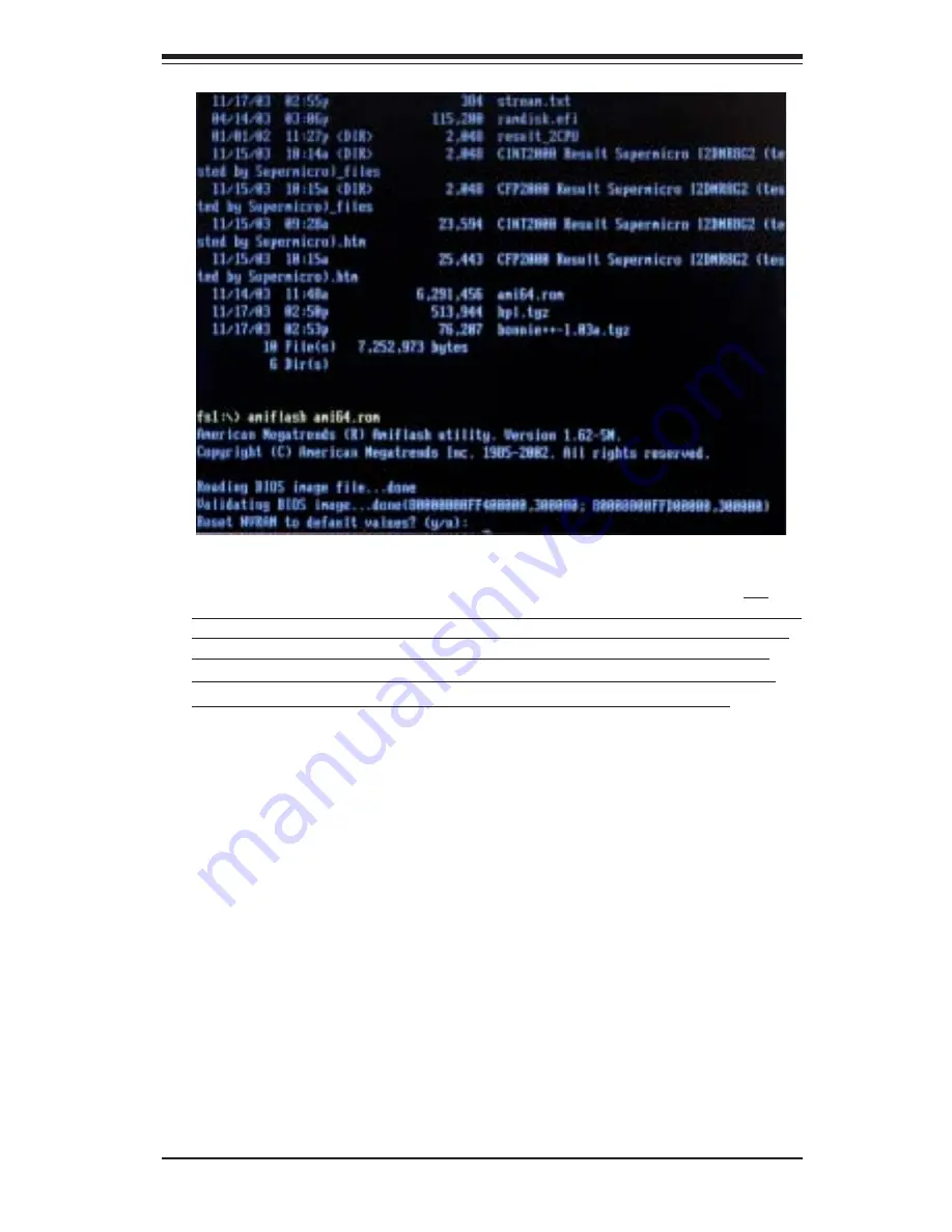
When asked "Reset NVRAM to default value? (y/n), type "y" at the

prompt, if you want to reset all default values after flashing the BIOS.(*y:
This will reset your NVRAM which typically resets your boot options in EFI to
manufacturer defaults. If you previously added options to boot from CDROM
or Windows, these will disappear after NVRAM is reset, and in this case

you will have to re-add the options. n: This will leave NVRAM alone, thus,

your boot options will still remain the same as before BIOS flashed.) Type

"n" at the prompt if you want to  keep the default values after BIOS flashing

as shown in the screen above.

After the BIOS Image file is loaded,  the following screen will appear:

9.

When asked "Proceed with flash update? (y/n), type "y" at the prompt

to update the BIOS. Type "n" at the prompt if you do not want to  update the

BIOS. If you type "y", the system will automatically update the BIOS file.

10.

After BIOS is updated, you will be asked "Reset CMOS to default

values (will be done during the next boot?) y/n? as shown in the screen

below. (*y: if you want to reset BIOS to manufacturer’s default settings

during the next boot,  or n: if you only want to update BIOS without resetting

it to manufacturer’s default settings.)

(*Please note that this reset will not affect EFI boot options.)

11.

Then, you will be asked "Reset the system? y/n? Type "y" at the

prompt if you want to automatically reboot the system.

Summary of Contents for SUPER i2DML-8G2

Page 1: ...SUPER i2DML 8G2 USER S MANUAL SUPER Revision 1 0 SUPER i2DML iG2...

Page 2: ...ILITY TO USE THIS PRODUCT OR DOCUMENTATION EVEN IF ADVISED OF THE POSSIBILITY OF SUCH DAMAGES IN PARTICULAR THE VENDOR SHALL NOT HAVE LIABILITY FOR ANY HARDWARE SOFTWARE OR DATA STORED OR USED WITH TH...

Page 3: ...fessionally installed Manual Organization Chapter 1 begins with a checklist of what should be included in your mainboard box describes the features specifications and performance of the motherboard an...

Page 4: ...1 2 Chipset Overview 1 10 1 3 Special Features 1 11 Recovery from AC Power Loss 1 11 1 4 PC Health Monitoring 1 11 1 5 ACPI Features 1 12 1 6 Power Supply 1 12 1 7 Super I O 1 13 Chapter 2 Installati...

Page 5: ...gs 2 23 Explanation of Jumpers 2 23 GLAN Enable Disable 2 24 CMOS Clear 2 24 SCSIEnable Disable 2 25 Watch Dog Enable Disable 2 26 VGA Enable Disable 2 26 2 7 Onboard Indicators 2 27 CCommon Debug Cod...

Page 6: ...ration 4 14 4 5 Security Setup 4 15 4 6 Exit Options 4 16 Chapter 5 Software Drivers and the OS Installation 5 1 Introduction to the EFI PLatform 5 1 5 2 Flash BIOS 5 2 5 3 Adding the CDROM Boot Optio...

Page 7: ...ovide you with the highest standards in quality and performance Check that the following items have all been included with your mother board If anything listed here is damaged or missing contact your...

Page 8: ...com Europe Address SuperMicro Computer B V Het Sterrenbeeld 28 5215 ML s Hertogenbosch The Netherlands Tel 31 0 73 6400390 Fax 31 0 73 6416525 Email sales supermicro nl General Information support sup...

Page 9: ...roduction 1 3 Introduction Figure 1 1 SUPER i2DML 8G2 i2DML iG2 Image Note The difference between the i2DML 8G2 and the i2DML iG2 There is LSI Ultra 320 SCSI on the i2DML 8G2 and there is no SCSI on t...

Page 10: ...VRM top ATI RAGE _XL bottom Front Panel CTLR J 3 5 J 3 6 J 3 7 GLAN Enable J 2 6 Speaker U62 1 Jumpers not noted are for testing purposes only SCSI Enable U S B 0 1 Fan7 82546 GLAN CTLR Fan8 S I O Fan...

Page 11: ...nel Connector Note 3 IDE1 J37 IDE2 J35 IDE1 2 Hard Disk Drive Connectors IPMI J26 IPMI 1 5 2 0 Connector PCI X J19 PCI X Bus 256 Pin Slot PW1 J20 PW2 J36 Power1 and Power2 24 Pin Connectors PWR Fault...

Page 12: ...Controller NIC 10 100 1000 Ethernet controller that provides two GLAN ports One I O Control Hub 4 ICH 4 component 4 USB ports 2 at the rear 2 headers at the front 2 IDE bus routed through the flex ca...

Page 13: ...Ms System overheat LED and control Chassis intrusion detection Thermal Control Overheat LED Indication Thermal control 8 Fan connectors ACPI Features Internal external modem ring On Control of power o...

Page 14: ...n Target Probe ITP port Joint Test Action Group JTAG boundary scan support through ITP or external source Core ratio programming via the SNC M Clock Buffering Embedded D2D converters I2 C Logic Includ...

Page 15: ...I FWH 3x1MB LPC Super I O LPC Bus COM1 COM2 PCIX 133 82546 2GLAN Ports PCIX 100 LSI SCSI PCI Slot UDMA100 IDE2 UDMA100 VXB Slot P64H2 1U Riser Card PCI Slot 1 PCI Slot 2 PCI Slot 3 2U Riser Card Hubli...

Page 16: ...or system bus supporting up to two processors and one Scalable Node Controller SNC with a maximum operating frequency of 200 MHz 400 MT s Rambus and SNC Interface the Interconnection between the SNC a...

Page 17: ...tion to change this setting The de fault setting is Last State 1 4 PC Health Monitoring This section describes the PC health monitoring features of the SUPER i2DML 8G2 i2DML iG2 All have an onboard Sy...

Page 18: ...stem is in the SoftOff state Note that external modem ring on can only be used with an SSI compliant power supply 1 6 Power Supply As with all computer products a stable power source is necessary for...

Page 19: ...power surges 1 7 Super I O The disk drive adapter functions of the Super I O provides two high speed 16550 compatible serial communication ports UARTs Each UART includes a 16 byte send receive FIFO a...

Page 20: ...1 14 Introduction SUPER i2DML 8G2 i2DML iG2 User s Manual Notes...

Page 21: ...emoving the board from the anti static bag Handle the board by its edges only do not touch its components periph eral chips memory modules or gold contacts When handling chips or modules avoid touchin...

Page 22: ...e fan Also do not place the motherboard on a conductive surface which can damage the BIOS battery and prevent the system from booting up Locate the following components which are included in the shipp...

Page 23: ...cure the retention mechanism onto the motherboard by screwing three 3 6 32 4 5MM screws into the mounting holes on the back of the motherboard 1 Place the retention mechanism on the motherboard 2 Scre...

Page 24: ...ounting holes in the chassis 3 Align the six mounting holes on the motherboard against the corre sponding mounting holes in the chassis 4 Screw six 6 6 32 8mm screws into the mounting holes on the ret...

Page 25: ...y to properly install and securely lock the Itanium 2 CPU onto the socket as shown below Use an M2 5 Hex Key to secure the CPU Notes Please refer to Chapter 1 Page 1 4 for the locations of CPU1 Socket...

Page 26: ...s on both edges of the CPU are fully seated in the Edge Connector and you hear a click Warning Unless the Signal Pins of the CPU are fully seated in the Edge Connector of the Power Pod the CPU will no...

Page 27: ...CPU w Power Pod as needed 3 Secure the Power Pod onto the motherboard with four 4 M3 screws 3 Locate four 4 M3 screws in the VRM 008 package Secure the Power Pod onto the motherboard with four 4 M3 s...

Page 28: ...s are aligned with those on the retention mechanism as shown in Figure 1 below 2 Screw in two diagonal screws ie the 1 and 2 screws until just snug do not fully tighten then do the same with the remai...

Page 29: ...PU if needed as shown in the Figure 4 Figure 4 The i2DML 8G2 iG2 with two heatsinks installed G Connecting the Power Supply to the motherboard and the Power Pods 1 Connect the 24 pin power connector f...

Page 30: ...starting with DIMM1 J16 DIMM2 J13 DIMM3 J11 DIMM4 J9 DIMM1 DIMM4 are the DIMM sockets colored in blue If four more DIMMs are used insert DIMM5 J15 DIMM6 J14 DIMM7 J12 and DIMM8 J10 into the slots DIMM...

Page 31: ...se it from the slot 2 4 I OPorts Control Panel Connectors The I O ports are color coded in conformance with the PC 99 specification See Figure 2 3 below for the colors and locations of the various I O...

Page 32: ...ions of the various control panel buttons and LED indicators Refer to the following section for descriptions and pin definitions Figure 2 4 Front Control Panel U66 Header Pins Power Button Overheat LE...

Page 33: ...S_ON 17 COM 18 COM 19 COM 20 Res NC 21 5V 22 5V 23 5V 24 COM Pin Number Definition 1 3 3V 2 3 3V 3 COM 4 5V 5 COM 6 5V 7 COM 8 PWR_OK 9 5VSB 10 12V 11 12V 12 3 3V 2 5 Connecting Cables Processor Power...

Page 34: ...efer to the table on the right for pin definitions Pin Number 15 16 Definition Vcc Control PWR_LED Pin Definitions U66 Power Button Overheat LED 1 NIC1 LED Reset Button 2 Power Fail LED HDD LED Power...

Page 35: ...ce Con troller LED connection for the GLAN port is located on pins 9 and 10 of U66 Attach the NIC LED cable to display network activity Refer to the table on the right for pin definitions NIC 2 LED Pi...

Page 36: ...Overheat OH LED Pin Definitions U66 Pin Number 7 8 Definition Vcc GND Power Button Overheat LED 1 NIC1 LED Reset Button 2 Power Fail LED HDD LED Power LED Reset Pwr Vcc Vcc Vcc Vcc Ground Ground 19 20...

Page 37: ...m connector and USB1 is the top connector of J1 See the table on the right for pin definitions Universal Serial Bus Pin Definitions Pin Number Definition 1 5V 2 P0 3 P0 4 Ground 5 N A Pin Number Defin...

Page 38: ...LSI SCSI Controller P64H ICH4 SIOH SNC VRM top VRM top FP CTLR R U S B 0 1 Fan7 GLAN CTLR Fan8 S I O S Fan4 Fan4 Fan3 3 3 P W R Fault COM2 6 2 5 DIMM5 1 Front Panel Universal Serial Bus Header An extr...

Page 39: ...1 LAN2 are located between Keyboard Mouse con nectors and the VGA connector This port accepts RJ45 type cables Pin Number 1 2 Definition Instrusion Ground Chassis Intrusion Pin Definitions J25 24Pin P...

Page 40: ...H ICH4 SIOH SNC VRM top VRM top FP CTLR R U S B 0 1 Fan7 GLAN CTLR Fan8 S I O S Fan4 Fan4 Fan3 3 3 P W R Fault COM2 6 2 5 DIMM5 1 Speaker Header The Speaker header is located on CN4 See the table on t...

Page 41: ...l ure This warning signal is passed through the PWR_LED pin on U66 to indicate of a power fail ure on the chassis See the table on the right for pin definitions Power Fault Pin Definitions U62 Pin Num...

Page 42: ...lled in the chassis If you only have a single power supply installed you should dis able this the default setting with CN5 to prevent false alarms See the table on the right for jumper settings The Al...

Page 43: ...nction of the connector Pin 1 is identified with a square solder pad on the printed circuit board See the motherboard layout pages for jumper locations Note On two pin jumpers Closed means the jumper...

Page 44: ...ns 2 3 Definition Enabled Disabled GLAN Enable Disable Jumper Settings J7 CMOS Clear JBT1 is not literally a jumper but con sists of two contact pads To clear the contents of CMOS short these pads tog...

Page 45: ...2 Fan6 Fan5 5 Fan6 Fan1 SMB P W Alarm Reset DIMM1 DIMM2 DIMM5 DIMM6 DIMM3 DIMM7 DIMM4 DIMM8 MRH D MRH D MRH D MRH D PCI X SCSI A L S I SCSI Controller P64H ICH4 SIOH SNC VRM top VRM top FP CTLR R U S...

Page 46: ...default po sition is on pins 1 and 2 to enable VGA See the table on the right for jumper settings Jumper Position 1 2 2 3 Definition Enabled default Disabled VGA Enable Disable Jumper Settings JV1 No...

Page 47: ...memory and SIOH found Off Off ICH4 found SCSI Activity LED i2DML 8G2 Only The SCSI Activity LED is located next to the LSI SCSI Controller When the SCSI Activity LED blinks it indicates that the SCSI...

Page 48: ...hen connecting the hard disk drive cable A red mark on a wire typically designates the location of pin 1 COM Port 1 J5 COM 2 Header J38 The COM Port 1 is located on J5 and the COM 2 Header is located...

Page 49: ...t Data 1 17 Host Data 0 19 GND 21 DRQ3 23 I O Write 25 I O Read 27 IOCHRDY 29 DACK3 31 IRQ14 33 Addr 1 35 Addr 0 37 Chip Select 0 39 Activity Pin Number Function 2 GND 4 Host Data 8 6 Host Data 9 8 Ho...

Page 50: ...3 24 25 26 27 28 29 30 31 32 33 34 Signal Names DB 12 DB 13 DB 14 DB 15 DB P1 DB 0 DB 1 DB 2 DB 3 DB 4 DB 5 DB 6 DB 7 DB P GROUND GROUND TERMPWR TERMPWR RESERVED GROUND ATN GROUND BSY ACK RST MSG SEL...

Page 51: ...m power requirement is 500W and above Also two 4 pin 12V 15A power connectors are required for CPU Power Pods VRMs 5 There is no BIOS Recovery function available Should a problem occur after flashing...

Page 52: ...2 The battery on your motherboard may be old Check to verify that it still supplies 3VDC If it does not replace it with a new one 3 If the above steps do not fix the Setup Configuration problem contac...

Page 53: ...ommended that you do not mix memory modules of different speeds and sizes Either 4 or 8 of identical DIMMs shall be installed 3 2 Technical Support Procedures Before contacting Technical Support pleas...

Page 54: ...ew drivers and programs that will greatly enhance your system We recommend that you review the CD and install the applications you need 3 4 Returning Merchandise for Service A receipt or copy of your...

Page 55: ...guide The Main BIOS setup menu screen has two main frames The left frame displays all the options that can be configured Grayed out options cannot be config ured Options in blue can be configured by...

Page 56: ...n by selecting the Main tab on the top of the screen The Main BIOS Setup screen is shown below AMI BIOS Version BIOS Built Date BIOS ID When you select the Main Setup the following items will be autom...

Page 57: ...P L3 Cache System Time System Date Use this option to change the system time and date Highlight System Time or System Date using the Arrow keys Enter new values through the keyboard Press the Tab key...

Page 58: ...Setup screen and sub menus are listed below Setup Warning When you first enter the Advanced Setup screen the Setup Warning will be displayed Please follow the instruction and set the correct value fo...

Page 59: ...nabled and Disabled The default setting for Serial Port1 is Enabled When Enabled is se lected for Serial Port1 the address for Serial Port1 will be automatically set to 2F8 IRQ3 The default setting fo...

Page 60: ...interrupt if block mode is not used Block mode allows transfers of up to 64 KB per interrupt Select Disabled to allow the data to be transferred from and to the device one sector at a time Select Auto...

Page 61: ...and UDMA4 The feature allows the BIOS to set ARMD Emulation type The options are Auto Floppy and Hard Disk ARMD Emulation Type allow the BIOS to use Single Word DMA mode 0 It has a data transfer rate...

Page 62: ...he op tions are Host Device Host and Device ATA PI 80Pin Cable Detection This item allows the user to configure the system s boot settings Boot Settings Configuration Quiet Boot Set this value to allo...

Page 63: ...Overheat Temperature This feature allows the user to set the temperature threshold Once the CPU temperature reaches the threshold the CPU Overheat Alarm will be set off to give warnings to the user C...

Page 64: ...e used in conjunction with the J31 jumper see Chapter 2 for details Options are Enabled and Disabled SCSI PCI Slot1 Frequency This setting allows the user to set the maximum PCI bus speed for the slot...

Page 65: ...ial port you want to use for console redirection You can set the value for this option to either COM1 or COM2 Serial Port Mode Select the baud rate you want the serial port to use for console redirect...

Page 66: ...es to the Remote System 115200 8 n 1 57600 8 n 1 19200 8 n 1 or 9600 8 n 1 Terminal Type Select the Terminal Type for console redirection You can set the value for this option to one of the following...

Page 67: ...allows the user to configure USB settings Legacy USB Support Select Enabled to enable the support for USB Legacy The options are Disabled Enabled and Auto Select Enabled to enable the USB Host Contro...

Page 68: ...latency to 192 PCI clock cycles Select 224 to set the PCI latency to 224 PCI clock cycles Select 248 to set the PCI latency to 248 PCI clock cycles Allocate IRQ to PCI VGA Set this value to allow or...

Page 69: ...ub menu You can use the sub menu to clear the user password 4 5 Security Settings AMI BIOS provides a Supervisor and a User password If you use both passwords the Supervisor password must be set first...

Page 70: ...Setup without making any permanent changes to the system configuration and reboot the computer Select Discard Changes and Exit from the Exit menu and press Enter Load Optimal Defaults To set this feat...

Page 71: ...Chapter 4 AMI BIOS 4 17 Discarding Changes Select this option and press Enter to discard all the changes and return to the BIOS Utility Program...

Page 72: ...4 18 SUPER i2DML 8G2 i2DML iG2 User s Manual Notes...

Page 73: ...t provides interface between the operating system and the computer firmware BIOS It abstracts system data specified in the system BIOS and translates it into an object oriented language that can be ea...

Page 74: ...to the files is www supermicro com 3 Connect the USB device to one of the USB ports See Page 1 4 for USB port locations 4 Boot up the system with the USB pen connected to a USB port The system will bo...

Page 75: ...3 Locate the USB device Ex ample The location of the USB device Example 6 At the Shell command prompt type Shell fsX X is the number of sector which your USB pen is located at This command will chang...

Page 76: ...hen the fsx directory appears type in the file name at the prompt fsx amiflash ami64 rom eg for the example shown above at the prompt type fs0 amiflash ami64 rom and press Enter as shown below Then th...

Page 77: ...shing as shown in the screen above After the BIOS Image file is loaded the following screen will appear 9 When asked Proceed with flash update y n type y at the prompt to update the BIOS Type n at the...

Page 78: ...a new description such as CDROM 6 When asked Enter Boot Option Data type A Ascii U Unicode N No boot Option Then press Enter 7 When asked Enter bootOption Data type Data will be stored as Unicode stri...

Page 79: ...is caused by un cleaned soldering 3 It is absolutely normal for the SCSI controller to take a while to detect the Hard drives since the firmware of the hard drives is built inside the EFI environment...

Page 80: ...you want to build RAID 1 in and hit the Enter Key Make sure that the LSI controller is enabled in both channels 00 channel A A high density connector located on the back of the board 01 channel B the...

Page 81: ...rs are usually communicated through a series of audible beeps The numbers on the fatal error list on the following page correspond to the number of beeps for the corresponding error All errors listed...

Page 82: ...Initial system memory and SIOH Off On Valid memory and SIOH found Off Off ICH4 found Common Debug Codes for the IA 64 systems are listed below Checkpoints CodeDescription Note The Debug Codes LEDs DS...

Page 83: ...zing the DMA controller performing the keyboard controller BAT test starting memory refresh and entering 4 GB flat mode next D3h Starting memory sizing next D4h Returning to real mode Executing any OE...

Page 84: ...d byte is written Next issuing the Pin 23 and 24 blocking and unblocking command 11h Next checking if End or Ins keys were pressed during power on Initializing CMOS RAM if the Initialize CMOS RAM in e...

Page 85: ...lay memory read write test next 32h The alternate display memory read write test passed Looking for alternate display retrace checking next 34h Video display checking is over Setting the display mode...

Page 86: ...a soft reset Displaying the first 64 KB memory size next 4Fh The memory size display has started The display is updated during the memory test Performing the sequential and random memory test next 50h...

Page 87: ...as completed Checking for a locked key next 84h Locked key checking is over Checking for a memory size mismatch with CMOS RAM data next 85h The memory size check is done Displaying a soft error and ch...

Page 88: ...before the Coprocessor test next 9Ch Required initialization before the Coprocessor test is over Initializing the Coprocessor next 9Dh Coprocessor initialized Performing any required initialization af...

Reviews: