background image

Chapter 2: Installation

2-7

2-6 Connecting 

Cables 

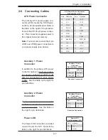
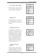
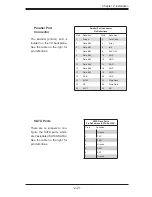
ATX Power Connector

The primary ATX power supply con-

nector (J1B1) meets the SSI (Super-

set ATX)  24-pin specifi cation. Refer to 

the table on the right for the pin defi ni-

tions of the ATX 24-pin power connec-

tor.  This connection supplies power to 

the chipset, fans and memory.  

Note:

 You must also connect the 8-pin 

JPW1 and JPW2 power connectors to 

your power supply (see below).

Required Connection

ATX Power 24-pin Connector

Pin Defi nitions (J1B1)

Pin#     Defi nition      Pin #      Defi nition

13

+3.3V

1

+3.3V

14

-12V

2

+3.3V

15

COM

3

COM

16

PS_ON

4

+5V

17

COM

5

COM

18

COM

6

+5V

19

COM

7

COM

20

Res (NC)

8

PWR_OK

21

+5V

9

5VSB

22

+5V

10

+12V

23

+5V

11

+12V

24

COM

12

+3.3V

Auxiliary 1 Power 
Connector 

In addition to the primary ATX power 

connector (above), the 8-pin proces-

sor power connector at JPW1 must 

also be connected to your power 

supply.  See the table on the right for 

pin defi nitions. 

Auxiliary 1 Power

 Connector

Pin Defi nitions (JPW1)

Pins                 Defi nition     

1 through 4

Ground

5 through 8

+12V

Auxiliary 2 Power 
Connector 

The 8-pin processor power connector 

at JPW2 must also be connected to 

your power supply.  See the table on 

the right for pin defi nitions. 

Required Connection

Auxiliary 2 Power

 Connector

Pin Defi nitions (JPW2)

Pins                 Defi nition     

1 & 2

Ground

3 & 4

+12V

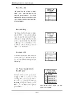
Power LED 

The Power LED connection is located 

on pins 15 and 16 of JF1.  Refer to the 

table on the right for pin defi nitions.  

Power LED

Pin Defi nitions (JF1)

Pin#     Defi nition     

15

Vcc

16

Control

Summary of Contents for H8QC8+

Page 1: ...H8QC8 H8QC8 H8QCE H8QCE USER S MANUAL Revision 1 0c ...

Page 2: ...OSSIBILITY OF SUCH DAMAGES IN PARTICULAR THE VENDOR SHALL NOT HAVE LIABILITY FOR ANY HARDWARE SOFTWARE OR DATA STORED OR USED WITH THE PRODUCT INCLUDING THE COSTS OF REPAIRING REPLACING INTEGRATING INSTALLING OR RECOVERING SUCH HARDWARE SOFTWARE OR DATA Any disputes arising between manufacturer and customer shall be governed by the laws of Santa Clara County in the State of California USA The Stat...

Page 3: ...ailed information about the chipset Chapter 2 begins with instructions on handling static sensitive devices Read this chapter when installing the processor s and memory modules and when installing the serverboard in a chassis Also refer to this chapter to connect the floppy and hard disk drives the parallel and serial ports the mouse and keyboard and the twisted wires for the power and reset button...

Page 4: ... System Block Diagram 1 10 1 2 Chipset Overview 1 11 1 3 PC Health Monitoring 1 12 1 4 Power Configuration Settings 1 13 1 5 Power Supply 1 14 1 6 Super I O 1 15 Chapter 2 Installation 2 1 Static Sensitive Devices 2 1 2 2 Processor and Heatsink Installation 2 2 2 3 Mounting the Serverboard into a Chassis 2 4 2 4 Installing Memory 2 4 2 5 I O Port and Control Panel Connections 2 6 2 6 Connecting Cab...

Page 5: ...er Settings 2 14 Explanation of Jumpers 2 14 CMOS Clear 2 14 I2 C to PCI X Slots 1 2 Enable Disable 2 15 I2 C to PCI X Slots 3 4 Enable Disable 2 15 SCSI Controller Enable Disable 2 15 SCSI Termination Enable Disable 2 16 VGA Enable Disable 2 16 3rd Power Supply Fail Signal Enable Disable 2 16 Watch Dog Enable Disable 2 17 JLAN Enable Disable 2 17 PCI X Slot Frequency Select 1 2 2 17 PCI X Slot Fr...

Page 6: ...the System s Setup Configuration 3 2 3 2 Technical Support Procedures 3 2 3 3 Frequently Asked Questions 3 3 3 4 Returning Merchandise for Service 3 4 Chapter 4 BIOS 4 1 Introduction 4 1 4 2 Main Menu 4 2 4 3 Advanced Settings Menu 4 2 4 4 Boot Menu 4 15 4 5 Security Menu 4 17 4 6 Exit Menu 4 17 Appendices Appendix A BIOS Error Beep Codes A 1 Appendix B BIOS POST Checkpoint Codes B 1 vi ...

Page 7: ... is damaged or missing contact your retailer Included with retail box only One 1 H8QC8 H8QCE serverboard One 1 IDE cable CBL 036 One 1 floppy cable CBL 022 Four 4 CPU backplates BKT 0004 Four 4 heatsink retention modules with eight 8 screws BKT 0005 One 1 COM port cable CBL 010 H8QC8 H8QCE only One 1 I O shield for chassis CSE PT7 H8QC8 H8QCE only One 1 air shroud with two 2 fans CSE PT0115 FAN 008...

Page 8: ...1 2 H8QC8 H8QCE User s Manual Figure 1 1 H8QC8 H8QCE Image Note The H8QC8 is shown The H8QCE shares the same layout but does not include SCSI controllers connectors or jumpers ...

Page 9: ...Chapter 1 Introduction 1 3 Figure 1 2 H8QC8 H8QCE Image Note The H8QC8 is shown The H8QCE shares the same layout but does not include SCSI controllers connectors or jumpers ...

Page 10: ... X 100 MHz Slot 3 PCI X 133 100 MHz Slot 4 PCI X 133 100 MHz Rage XL Graphics JA1 SATA3 SATA2 SATA1 SATA0 Slot 5 PCI E x8 BIOS COM2 AIC 7902W HT Connector Slot 6 PCI E x8 82546 JLAN2 HT Connector J3 USB0 1 FAN6 Battery JPG1 JPL1 JI2 C3 JI2 C4 J16 JPA2 J3P JPA3 JL1 JPA1 JP2 J34 J12 JP1 JWOR JWD JUSB2 3 JWOL JSMB JI2 C2 JI2 C1 FAN5 FAN4 CPU1 FAN3 CPU2 FAN2 FAN1 JOH1 JAR JF1 JF2 Note Jumpers not indi...

Page 11: ...ystem CPU Fan Headers Floppy Floppy Disk Drive Connector IDE 1 IDE 2 IDE 1 IDE 2 Connectors J1B1 24 Pin ATX Power Connector J3 PS 2 Keyboard Mouse Ports J12 J34 HT Connectors J16 I2 C Header for Power Supply JA1 JA2 U320 SCSI Channel A B Connector JAR 3rd Power Supply Alarm Reset Header JF1 Front Panel Connector JF2 Onboard Speaker Keylock Power LED JIPMI IPMI Daughter Card Slot JL1 Chassis Intrus...

Page 12: ...I Super IO JA2 nForce Pro 2200 CK804 AMD 8132 Rage XL Graphics JA1 SATA3 SATA2 SATA1 SATA0 BIOS AIC 7902W HT Connector Slot 6 PCI E x8 82546 JLAN2 J3 USB0 1 FAN6 Battery JPG1 JPL1 J16 JPA2 J3P JPA3 JL1 JPA1 JP2 J34 JP1 JWOR JWD JUSB2 3 JWOL JSMB FAN5 FAN4 CPU1 FAN3 CPU2 FAN2 FAN1 JOH1 JAR JF1 JF2 Note Jumpers not indicated are for test purposes only The H8QCE shares the same layout but does not in...

Page 13: ...nnectors J1B1 24 Pin ATX Power Connector J3 PS 2 Keyboard Mouse Ports J16 I2 C Header for Power Supply J34 HT Connectors JA1 JA2 U320 SCSI Channel A B Connector JAR 3rd Power Supply Alarm Reset Header JF1 Front Panel Connector JF2 Onboard Speaker Keylock Power LED JIPMI IPMI Daughter Card Slot JL1 Chassis Intrusion Header JLAN1 2 Gigabit Ethernet RJ45 Ports JOH1 Overheat Warning Header JPW1 Auxili...

Page 14: ...xpress x8 slots Two 2 PCI X 133 100 MHz slots Two 2 PCI X 100 MHz slots one with ZCR card support H8QC8 H8QCE One 1 PCI Express x8 slot BIOS 8 Mb Firmware Hub AMIBIOS Flash ROM APM 1 2 DMI 2 3 PCI 2 2 ACPI 1 0 ACPI 2 0 is BIOS supported SMBIOS 2 3 Plug and Play PnP PC Health Monitoring Onboard voltage monitors for four CPU cores Hyper Transport 1 2V memory banks 2 5V nVidia 2200 chipset 1 5V Fan s...

Page 15: ...20 SCSI H8QC8 and H8QC8 only Two 2 UltraDMA133 100 IDE ports One 1 floppy port interface up to 2 88 MB Two 2 Fast UART 16550 compatible serial ports one only on H8QC8 and H8QCE Intel 82546GB Ethernet controller supports two Gigabit LAN ports ATI Rage 8 MB XL graphics chip PS 2 mouse and PS 2 keyboard ports Four 4 USB Universal Serial Bus 2 0 ports headers Other Wake on Ring JWOR Wake on LAN JWOL Ch...

Page 16: ...nk 1 GHz Slot 2 PCI X 100 MHz Dual SCSI Channels Gb LAN Ports 2 SATA Ports 4 UDMA133 USB Ports 4 LPC I O FWH Kybd Mouse FDD Parallel Port COM Ports AMD OpteronTM CPU 1 AMD OpteronTM CPU 3 AMD OpteronTM CPU 2 DIMM 1B DIMM2A DIMM2B DIMM1A DIMM 1B DIMM 2A DIMM 2B 16 x 16 HT link 1 GHz 128 bit data 16 bit ECC 16 x 16 HT link 1 GHz Slot 1 PCI X 100 MHz Slot 3 PCI X 100 MHz Slot 4 PCI X 100 MHz PCI X CH...

Page 17: ... The IPMI and LPC buses also connect to the 2200 8132 HyperTransport PCI X Tunnel This hub includes AMD specific technology that provides two PCI X bridges with each bridge supporting a 64 bit data bus as well as separate PCI X operational modes and independent transfer rates Each bridge supports up to five PCI mas ters that include clock request and grant signals It also interfaces directly with th...

Page 18: ...hese voltage levels are all displayed in BIOS Fan Status Monitor with Firmware Software Speed Control The PC health monitor can check the RPM status of the cooling fans The onboard fans are controlled by thermal management via BIOS CPU Overheat Fan Fail LED and Control This feature is available when the user enables the CPU overheat Fan Fail warning function in the BIOS This allows the user to defi...

Page 19: ... function as a system suspend button When the user depresses the power button the system will enter a SoftOff state The monitor will be suspended and the hard drive will spin down Depressing the power button again will cause the whole system to wake up Dur ing the SoftOff state the ATX power supply provides power to keep the required circuitry in the system alive In case the system malfunctions an...

Page 20: ...t is recommended that you also install a power surge protector to help avoid problems caused by power surges Warning To prevent the possibility of explosion do not use the wrong type of onboard CMOS battery or install it upside down Wake On Ring Header JWOR Wake up events can be triggered by a device such as the external modem ringing when the system is in the SoftOff state Note that external mode...

Page 21: ...rts serial infrared communication Each UART in cludes a 16 byte send receive FIFO a programmable baud rate generator complete modem control capability and a processor interrupt system Both UARTs provide legacy speed with baud rate of up to 115 2 Kbps as well as an advanced speed with baud rates of 250 K 500 K or 1 Mb s which support higher speed modems The Super I O supports one PC compatible prin...

Page 22: ...ss SuperMicro Computer B V Het Sterrenbeeld 28 5215 ML s Hertogenbosch The Netherlands Tel 31 0 73 6400390 Fax 31 0 73 6416525 Email sales supermicro nl General Information support supermicro nl Technical Support rma supermicro nl Customer Support Asia Pacific Address SuperMicro Taiwan 4F No 232 1 Liancheng Rd Chung Ho 235 Taipei County Taiwan R O C Tel 886 2 8226 3990 Fax 886 2 8226 3991 Web Site ...

Page 23: ...ard and peripherals back into their antistatic bags when not in use For grounding purposes make sure your computer chassis provides excellent conductivity between the power supply the case the mounting fasteners and the serverboard Use only the correct type of CMOS onboard battery as specified by the manufac turer Do not install the CMOS onboard battery upside down which may result in a possible ex...

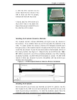
Page 24: ...ket Triangles Installing the CPU Backplates Four CPU backplates BKT 0004 are included in the retail box The backplates prevent the CPU area of the serverboard from bending and provide a base for at taching the heatsink retention modules To install begin by peeling off the release paper to expose the adhesive On the underside of the serverboard locate the two holes on either side of the CPU socket ...

Page 25: ...kets Installing the Heatsink Retention Modules Four heatsink retention modules BKT 0005 and eight screws are included in the retail box Once installed these are used to help attach the heatsinks to the CPUs To install position the module so that the CPU backplate standoffs insert through the holes on the heatsink retention module and the four feet on the module contact the serverboard Secure the r...

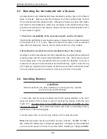
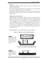
Page 26: ...oles with the raised metal standoffs in the tray Insert screws into all the mounting holes in the serverboard that line up with the standoffs Then use a screwdriver to secure the serverboard to the mainboard tray tighten until just snug if too tight you might strip the threads Metal screws provide an electrical contact to the serverboard ground to provide a continuous ground for the system 2 4 Ins...

Page 27: ...cent slots at a time with memory modules of the same size and type will result in interleaved 128 bit memory which is faster than non interleaved 64 bit memory Optimizing memory performance With the mandatory four processors installed it is better to spread out pairs of DIMMs across all four CPU memory banks than filling up one CPU memory bank while leaving any others empty For example if you were ...

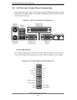
Page 28: ...s Figure 2 3 I O Port Locations and Definitions Front Control Panel JF1 contains header pins for various front control panel connectors See Figure 2 4 for the pin definitions of the various connectors Refer to Section 2 6 for details Figure 2 4 JF1 Front Control Panel Header JF1 NC x key Vcc Vcc Vcc Vcc Vcc Vcc Reset Button Power Button NC x key Power LED HDD LED NIC1 NIC2 OH Fan Fail LED Power Fail...

Page 29: ...R_OK 21 5V 9 5VSB 22 5V 10 12V 23 5V 11 12V 24 COM 12 3 3V Auxiliary 1 Power Connector In addition to the primary ATX power connector above the 8 pin proces sor power connector at JPW1 must also be connected to your power supply See the table on the right for pin definitions Auxiliary 1 Power Connector Pin Definitions JPW1 Pins Definition 1 through 4 Ground 5 through 8 12V Auxiliary 2 Power Connector...

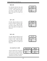
Page 30: ...l ler LED connection is located on pins 9 and 10 of JF1 Attach the NIC2 LED cable to display network activity Refer to the table on the right for pin definitions OH Fan Fail LED Pin Definitions JF1 Pin Definition 7 Vcc 8 Control NIC1 LED Pin Definitions JF1 Pin Definition 11 Vcc 12 NIC1 Active NIC2 LED Pin Definitions JF1 Pin Definition 9 Vcc 10 NIC2 Active HDD LED The HDD IDE Hard Disk Drive LED connect...

Page 31: ...nd 2 of JF1 Mo mentarily contacting both pins will power on off the system This button can also be configured to function as a suspend button see the Power Button Mode setting in BIOS To turn off the power when set to suspend mode depress the button for at least 4 seconds Refer to the table on the right for pin definitions Universal Serial Bus Ports USB0 1 Two Universal Serial Bus ports USB2 0 are l...

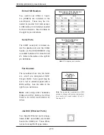
Page 32: ...M2 port These Ether net ports accept RJ45 type cables Note NC indicates no connection Serial Port Pin Definitions COM1 COM2 Pin Definition Pin Definition 1 DCD 6 DSR 2 RXD 7 RTS 3 TXD 8 CTS 4 DTR 9 RI 5 Ground 10 NC Fan Header Pin Definitions FAN1 9 Pin Definition 1 Ground Black 2 12V 9V Red 3 Tachometer Extra USB Headers Two additional USB2 0 head ers USB2 3 are included on the serverboard These may b...

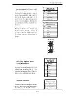
Page 33: ...n 9 See the tables on the right for pin definitions and below right for pin locations Note The speaker connector pins are for use with an external speaker If you wish to use the onboard speaker you should close pins 5 and 7 with a jumper Pwr LED Keylock Connector Pin Definitions JF2 Pin Definition 2 Vcc 4 Vcc 6 Vcc 8 Keylock 10 Ground Speaker Connector Pin Definitions JF2 Pin Definition 1 Red wire spea...

Page 34: ...k 2 Wake up Wake On LAN Pin Definitions JWOL Pin Definition 1 5V Standby 2 Ground 3 Wake up Overheat LED Connect an LED to the JOH header to provide warning of chassis overheat ing See the table on the right for pin definitions Overheat LED Pin Definitions JOH Pin Definition 1 3 3V 2 OH Active 3rd Power Supply Alarm Reset Header Connect a cable from your power supply to JAR to provide you with warning ...

Page 35: ... Headers Four additional fan headers desig nated nFAN1 through nFAN4 are included on the serverboard On the H8QC8 H8QCE nFAN1 and nFAN2 should be connected to the heatsinks on the CK804 and 8132 chipset chips On the H8QC8 H8QCE nFAN3 and nFAN4 should be con nected to the heatsinks that are used with the air shroud See the table on the right for pin definitions Additional Fan Header Pin Definitions n...

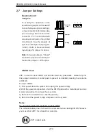
Page 36: ...se the PW_ON connector to clear CMOS The onboard battery does not need to be removed when clearing CMOS however you must short JBT1 for at least four seconds JBT1 contact pads 2 7 Jumper Settings Explanation of Jumpers To modify the operation of the serverboard jumperscanbeusedto choose between optional settings Jumperscreateshortsbetweentwo pins to change the function of the connector Pin 1 is id...

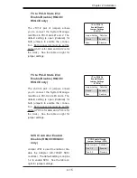
Page 37: ...H8QCE only The JI2 C3 4 pair of jumpers allows you to connect the System Manage ment Bus to PCI X slots 3 and 4 The default setting is open disabled for both jumpers to enable the connec tion Both connectors must be set the same JI2 C3 is for data and JI2 C4 is for the clock See the table on right for jumper settings I2 C to PCI 3 4 Enable Disable Jumper Settings JI2 C3 4 Jumper Setting Definition ...

Page 38: ...JPG1 allows you to enable or disable the VGA port The default position is on pins 1 and 2 to enable VGA See the table on the right for jumper set tings VGA Enable Disable Jumper Settings JPG1 Jumper Setting Definition Pins 1 2 Enabled Pins 2 3 Disabled 3rd Power Supply Fail Signal Enable Disable The system can notify you in the event of a power supply failure This feature assumes that three redunda...

Page 39: ... needs to write their own application software in or der to disable the Watch Dog timer JLAN Enable Disable Change the setting of jumper JPL1 to enable or disable the JLAN1 and JLAN2 Gb Ethernet ports See the table on the right for jumper settings The default setting is enabled JLAN1 2 Enable Disable Jumper Settings JPL1 Jumper Setting Definition Pins 1 2 Enabled Pins 2 3 Disabled PCI X Slot Freque...

Page 40: ...ght for the functions as sociated with the activity speed LED JLAN LED Connection Speed Indicator LED Color Definition Off 10 MHz Green 100 MHz Amber 1 GHz PCI X Slot Frequency Select H8QC8 H8QCE only Jumper JPXB1 is are used to set the speed of PCI X slots 3 and 4 respectively The recommended de fault setting is open for Auto See the table on the right for jumper settings PCI X Slot 3 4 Frequency ...

Page 41: ...l cable should be used to take advantage of the speed this new technology offers The blue connector connects to the onboard IDE connector interface and the other connector s to your hard drive s Consult the documentation that came with your disk drive for details on actual jumper locations and settings for the hard disk drive Floppy Drive Connector Pin Definitions Floppy Pin Definition Pin Definition...

Page 42: ...st Data 7 4 Host Data 8 5 Host Data 6 6 Host Data 9 7 Host Data 5 8 Host Data 10 9 Host Data 4 10 Host Data 11 11 Host Data 3 12 Host Data 12 13 Host Data 2 14 Host Data 13 15 Host Data 1 16 Host Data 14 17 Host Data 0 18 Host Data 15 19 Ground 20 Key 21 DRQ3 22 Ground 23 I O Write 24 Ground 25 I O Read 26 Ground 27 IOCHRDY 28 BALE 29 DACK3 30 Ground 31 IRQ14 32 IOCS16 33 Addr1 34 Ground 35 Addr0 ...

Page 43: ...XP 7 Ground Parallel Port Connector The parallel printer port is located on the I O backplane See the table on the right for pin definitions Parallel Port Connector Pin Definitions Pin Definition Pin Definition 1 Strobe 2 Auto Feed 3 Data Bit 0 4 Error 5 Data Bit 1 6 Init 7 Data Bit 2 8 SLCT IN 9 Data Bit 3 10 GND 11 Data Bit 4 12 GND 13 Data Bit 5 14 GND 15 Data Bit 6 16 GND 17 Data Bit 7 18 GND 19 A...

Page 44: ... DB 7 47 DB 7 14 DB P 48 DB P 15 Ground 49 Ground 16 DIFFSENS 50 Ground 17 TERMPWR 51 TERMPWR 18 TERMPWR 52 TERMPWR 19 Reserved 53 Reserved 20 Ground 54 Ground 21 ATN 55 ATN 22 Ground 56 Ground 23 BSY 57 BSY 24 ACK 58 ACK 25 RST 59 RST 26 MSG 60 MSG 27 SEL 61 SEL 28 C D 62 C D 29 REQ 63 REQ 30 I O 64 I O 31 DB 8 65 DB 8 32 DB 9 66 DB 9 33 DB 10 67 DB 10 34 DB 11 68 DB 11 SCSI Connectors H8QC8 H8QC...

Page 45: ...install the driver during the OS installation Note the SATA RAID driver is supported by Windows 2000 and XP only Building a Driver Diskette You must first build a driver diskette from the CD ROM that was included with the system You will have to create this disk on a computer that is already running and with the OS installed Insert the CD into your CD ROM drive and start the system A display as sho...

Page 46: ...indow on the right which lists all drives that are to become part of the RAID array Once you have finished selecting the drives and type of RAID you wish to use for your RAID array press the F7 key You will be prompted to verify your choice if you want to continue with your choices select Yes Note that selecting Yes will clear all previous data from the drives you selected to be a part of the array...

Page 47: ...Chapter 2 Installation 2 25 Figure 2 5 Driver Installation Screen ...

Page 48: ...2 26 H8QC8 H8QCE User s Manual Notes ...

Page 49: ...d on cards 5 Install CPUs and heatsinks making sure it is fully seated and connect the in ternal chassis speaker and the power LED to the serverboard Check all jumper settings as well 6 Use the correct type of onboard CMOS battery as recommended by the manufac turer To avoid possible explosion do not install the CMOS battery upside down No Power 1 Make sure that no short circuits exist between the...

Page 50: ...ies 2 The battery on your serverboard may be old Check to verify that it still supplies 3VDC If it does not replace it with a new one 3 If the above steps do not fix the setup configuration problem contact your vendor for repairs 3 2 Technical Support Procedures Before contacting Technical Support please take the following steps Also note that as a serverboard manufacturer we do not sell directly to...

Page 51: ...dated BIOS files are located on our web site Please check our BIOS warning message and the information on how to update your BIOS on our web site Also check the current BIOS revision and make sure it is newer than your current BIOS before downloading Select your mainboard model on the web page and download the corresponding BIOS file to your computer Unzip the BIOS update file in which you will find t...

Page 52: ...eturning Merchandise for Service A receipt or copy of your invoice marked with the date of purchase is required be fore any warranty service will be rendered You can obtain service by calling your vendor for a Returned Merchandise Authorization RMA number When returning to the manufacturer the RMA number should be prominently displayed on the outside of the shipping carton and mailed prepaid or ha...

Page 53: ... F1 F2 etc Each main BIOS menu option is described in this manual The Main BIOS screen has two main frames The left frame displays all the options that can be configured Grayed out options cannot be configured The right frame displays the key legend Above the key legend is an area reserved for a text mes sage When an option is selected in the left frame it is highlighted in white Often a text messag...

Page 54: ...Y MM DD YYYY format The time is entered in HH MM SS format Please note that time is in a 24 hour format For example 5 30 A M appears as 05 30 00 and 5 30 P M as 17 30 00 4 3 Advanced Settings Menu CPU Configuration Sub Menu GART Error Reporting This setting is used for testing only MTRR Mapping This determines the method used for programming CPU MTRRs when 4 GB or more memory is present The options...

Page 55: ...nsferred from and to the device one sec tor at a time Select Auto to allows the data transfer from and to the device occur multiple sectors at a time if the device supports it The options are Auto and Disabled PIO Mode PIO Programmable I O mode programs timing cycles between the IDE drive and the programmable IDE controller As the PIO mode increases the cycle time decreases The options are Auto 0 ...

Page 56: ...Reporting Technology SMART can help predict impending drive failures Select Auto to allow BIOS to auto detect hard disk drive support Select Disabled to prevent AMI BIOS from using the S M A R T Select Enabled to allow AMI BIOS to use the S M A R T to support hard drive disk The options are Disabled Enabled and Auto 32 Bit Data Transfer Select Enabled to activate the function of 32 Bit data transf...

Page 57: ...st boot device as being P ATA or S ATA Configuration nVidia RAID ROM RAID Option ROM This setting is used to Enable or Disable the nVidia ROM Floppy Configuration Floppy A Move the cursor to these fields via up and down arrow keys to select the floppy type The options are Disabled 360 KB 5 1 4 1 2 MB 5 1 4 720 KB 3 1 44 MB 3 and 2 88 MB 3 Floppy B Move the cursor to these fields via up and down arrow k...

Page 58: ...are Yes and No Palette Snooping Select Enabled to inform the PCI devices that an ISA graphics device is installed in the system in order for the graphics card to function properly The options are Enabled and Disabled PCI IDE BusMaster Set this value to allow or prevent the use of PCI IDE busmastering Select Enabled to allow AMI BIOS to use PCI busmaster for reading and writing to IDE drives The op...

Page 59: ... as its I O port address and IRQ 4 for the interrupt address The options are Disabled 3F8 IRQ4 3E8 IRQ4 and 2E8 IRQ3 Serial Port2 Address This option specifies the base I O port address and Interrupt Request address of serial port 2 Select Disabled to prevent the serial port from accessing any system resources When this option is set to Disabled the serial port physically becomes unavailable Select...

Page 60: ...r the parallel port The options are IRQ5 and IRQ7 Chipset Menu North Bridge Configuration Memory Configuration Memclock Mode This setting determines how the memory clock is set Auto has the memory clock by code and Limit allows the user to set a standard value MCT Timing Mode Sets the timing mode for memory Options are Auto and Manual User Configuration Mode Options are Auto and Manual Bank Interleav...

Page 61: ...ptions are Enabled and Disabled MCA DRAM ECC Logging When Enabled MCA DRAM ECC logging and reporting is enabled Options are Enabled and Disabled ECC Chipkill Allows the user to enabled ECC Chipkill Options are Enabled and Disabled DRAM Scrub Redirect Allows system to correct DRAM ECC errors immediately even with background scrubbing on Options are Enabled and Disabled DRAM BG Scrub Corrects memory...

Page 62: ...r to select which CPU Node s timing parameters memory clock etc to display Options are CPU Node 0 CPU Node1 CPU Node 2 and CPU Node 3 South Bridge Configuration CPU Spread Spectrum This setting is used to enable spread spectrum for the CPU Options are Dis abled and Center Spread SATA Spread Spectrum This setting is used to enable spread spectrum for the SATA Options are Dis abled and Down Spread PC...

Page 63: ...e pointer to R X SDT pointer lists Options are Enabled and Disabled Headless Mode Enable this setting to activate the Headless Operation Mode through ACPI The options are Enabled and Disabled Power Menu Power Button Mode Allows the user to change the function of the power button Options are On Off and Suspend Restore on AC Power Loss This setting allows you to choose how the system will react when...

Page 64: ...MHz 400 MHz 600 MHz 800 MHz and 1 GHz CPU0 PCI X0 HT Link Width The HT link will run at the width specified in this setting Options are Auto 2 bit 4 bit 8 bit and 16 bit CPU HT_Slot HT1 Link Speed This setting becomes accessible when a card is installed to the J34 HT slot The HT link will run at the speed specified in this setting if it is slower than or equal to the system clock and if the board is...

Page 65: ...e Access USB Configuration This screen will display the module version and all USB enabled devices USB Controller Support Enable the controller for your USB ports Options are Disabled USB 1 1 only and USB 1 1 USB 2 0 Legacy USB Support Select Enabled to enable the support for USB Legacy Disable Legacy support if there are no USB devices installed in the system The options are Disabled Enabled and A...

Page 66: ...mperature CPU4 Temperature CPU1 Vcore CPU2 Vcore CPU3 Vcore CPU4 Vcore 5Vin 12Vin 12Vcc V and Battery Voltage System Fan Monitor Fan Speed Control Modules This feature allows the user to determine how the system will control the speed of the onboard fans If the option is set to Server Mode the fan speed will vary between full speed 12V and reduced speed 9V based on system temperature Selecting to ...

Page 67: ...ystem to force a third party BIOS to display during system boot Select Keep Current to allow the computer system to display the BIOS information during system boot Boot up Num Lock Set this to On to allow the Number Lock setting to be modified during boot up The options are On and Off PS 2 Mouse Support This setting is to specify PS 2 mouse support The options are Auto Enabled and Disabled Wait for...

Page 68: ...ure allows the user to specify the Boot sequence from available hard disk drives Removable Drives This feature allows the user to specify the Boot sequence from available remov able drives 1st Drive Specifies the boot sequence for the 1st Removable Drive The options are 1st Floppy Drive and Disabled OS Installation Specify the OS used Options are Linux and Other Onboard SCSI Host RAID Use this sett...

Page 69: ...or virus issues a Disk Format command or attempts to write to the boot sector of the hard disk drive The options are Enabled and Disabled 4 6 Exit Menu Select the Exit tab from AMI BIOS Setup Utility screen to enter the Exit BIOS Setup screen Save Changes and Exit When you have completed the system configuration changes select this option to leave BIOS Setup and reboot the computer so the new syste...

Page 70: ...atically load the Optimal Defaults as the BIOS Settings The Optimal settings are designed for maximum system performance but may not work best for all computer applications Load Fail Safe Defaults To set this feature select Load Fail Safe Defaults from the Exit menu and press Enter The Fail Safe settings are designed for maximum system stability but not maximum performance ...

Page 71: ...ually communicated through a series of audible beeps The numbers on the fatal error list on the following page correspond to the number of beeps for the corresponding error All errors listed with the exception of Beep Code 8 are fatal errors POST codes may be read on the debug LEDs located beside the LAN port on the serverboard backplane See the description of the Debug LEDs LED1 and LED2 in Chapt...

Page 72: ...A 2 H8QC8 H8QCE User s Manual Notes ...

Page 73: ...s are listed in order of execution Checkpoint Code Description D0h The NMI is disabled Power on delay is starting Next the initialization code check sum will be verified D1h Initializing the DMA controller performing the keyboard controller BAT test starting memory refresh and entering 4 GB flat mode next D3h Starting memory sizing next D4h Returning to real mode Executing any OEM patches and settin...

Page 74: ...rred while reading the floppy drive in drive A F0h Next searching for the AMIBOOT ROM file in the root directory F1h The AMIBOOT ROM file is not in the root directory F2h Next reading and analyzing the floppy diskette FAT to find the clusters occupied by the AMIBOOT ROM file F3h Next reading the AMIBOOT ROM file cluster by cluster F4h The AMIBOOT ROM file is not the correct size F5h Next disabling interna...

Page 75: ...d during power on Initializing CMOS RAM if the Initialize CMOS RAM in every boot AMIBIOS POST option was set in AMIBCP or the End key was pressed 12h Next disabling DMA controllers 1 and 2 and interrupt controllers 1 and 2 13h The video display has been disabled Port B has been initialized Next initializing the chipset 14h The 8254 timer test will begin next 19h Next programming the flash ROM 1Ah T...

Page 76: ...L general devices next if present See the last page of this chapter for additional information 39h Displaying bus initialization error messages See the last page of this chapter for additional information 3Ah The new cursor position has been read and saved Displaying the Hit DEL mes sage next 3Bh The Hit DEL message is displayed The protected mode memory test is about to start 40h Preparing the de...

Page 77: ... was adjusted for relocation and shadowing Clearing the Hit DEL message next 59h The Hit DEL message is cleared The WAIT message is displayed Starting the DMA and interrupt controller test next 60h The DMA page register test passed Performing the DMA Controller 1 base register test next 62h The DMA controller 1 base register test passed Performing the DMA controller 2 base register test next 65h T...

Page 78: ...ontrol and has now returned control to BIOS POST Perform ing any required processing after the option ROM returned control 99h Any initialization required after the option ROM test has completed Configuring the timer data area and printer base address next 9Ah Set the timer and printer base addresses Setting the RS 232 base address next 9Bh Returned after setting the RS 232 base address Performing ...

Page 79: ...0 option ROM had control next Aah Initialization after E000 option ROM control has completed Displaying the system configuration next Abh Uncompressing the DMI data and executing DMI POST initialization next B0h The system configuration is displayed B1h Copying any code to specific areas 00h Code copying to specific areas is done Passing control to INT 19h boot loader next ...

Page 80: ...B 8 H8QC8 H8QCE User s Manual Notes ...

Reviews: