


Hardware and layout
UM1079
20/38
DocID018789 Rev 4
The Q13 output of the counter allows connecting the 1 KW resistor when the current I
DD
becomes very low.
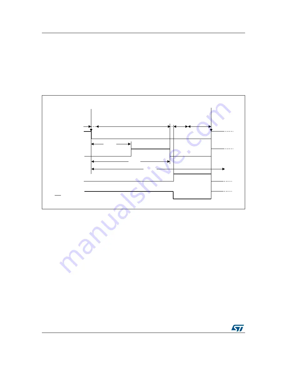
Figure 11
shows how the counter and the FET transistor 1 of U20 ensure that, 150 ms after
IDD_CNT_EN falling edge, the shunt resistor R22 is connected between VDD_MCU and
the power supply to reduce the measurement range to 60
μ
A for the full scale. Then after
another 150 ms required for current stabilization, R22 is shorted, the I
DD
measurement is
stored in C13, and the MCU is woken up. After wakeup, the MCU measures the I
DD
current
corresponding to the Low-power mode stored in C13.
Figure 11. Low I
DD
range measurement timing diagram
4.7.3 I
BIAS
current measurement procedure
In low I
DD
range mode, the bias current of the operational amplifier input (U5 pin 4) is not
negligible compared to I
DD
current (typical I
BIAS
is ~240 nA). To obtain a reliable I
DD
measurement, it is mandatory to subtract the bias current from the low I
DD
current value
since this current is not sunk by the MCU. I
BIAS
is measured during production test and
stored in the MCU data EEPROM. The discovery demonstration software uses this value to
display the correct I
DD
.
The procedure for I
BIAS
measurement implemented in the demonstration software is:
1.
Power off the board (disconnect the USB cable).
2. Set
JP1
OFF.
3. Push down B1 (USER button), power on the board from the USB.
4. Wait at least 1 second before releasing B1. The LCD displays the I
BIAS
measurement.
5. Power off the board (disconnect the USB cable).
6. Set JP1 ON. The I
BIAS
value is stored in data EEPROM. The bias current is then
subtracted from the I
DD
measured in I
DD
range mode.
069
,''B&17B(1
4 /2:B32:(5B(1
8SLQ
4 ,''B:$.(83
4 8SLQ
5XQPRGH
/RZSRZHUPRGH
:DNHXS
,''
PHDVXUHPHQW
&OHDU
8FRXQWHU
8FRXQWHUHQDEOHG
PV
PV
PV


