background image

AN2339

Development and debugging tool support

15/20

5.2.1 ETM 

Interface 

pins

The ETM interface pins consist of the following signals:
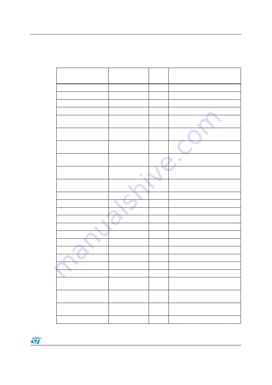
         

Table 3.

ETM interface signals

Target board 

STR91x

name

Signal 

pin 

Description

NC 

Not used

1

No Connect

NC 

Not used

3

No Connect

VSSQ

VSSQ

5

Signal ground

DBGRQ Not 

used

7

Debug 

request

NSRST nRSTIN

9

Open-collector output from the run 

control to the target system reset.

TDO

JTDO

11

Open-collector output from the run 

control to the target system reset

RTCK

JRTCK

13

Return test clock from the target JTAG 

port

TCK

JTCK

15

Test clock to the run control unit from 

the JTAG port

TMS

JTMS

17

Test mode select from run control to 

the JTAG port

TDI

JTDI

19

Test data input from run control to the 

JTAG port

NTRST

JNTRST

21

Active-low JTAG reset

Port A TRACEPKT[15]

Not used

23

The trace packet port

Port A TRACEPKT[14]

Not used

25

The trace packet port

Port A TRACEPKT[13]

Not used

27

The trace packet port

Port A TRACEPKT[12]

Not used

29

The trace packet port

Port A TRACEPKT[11]

Not used

31

The trace packet port

Port A TRACEPKT[10]

Not used

33

The trace packet port

Port A TRACEPKT[9]

Not used

35

The trace packet port

Port A TRACEPKT[8]

Not used

37

The trace packet port

NC

Not used

2

No Connect

NC

Not used

4

No Connect

Port A TRACECLK

ETM_TRCLK

6

Clocks trace data on rising edge or 

both edges

DBGACK

Not used

8

Debug acknowledge from the test 

chip, high


when in debug state

EXTRIG

ETM_EXTRIG

10

Optional external trigger signal to the 

Embedded trace Macrocell (ETM)

VTRef

VDDQ

12

Signal level reference

Summary of Contents for STR91 Series

Page 1: ...rm signal cycle DSP instructions good for speech processing audio algorithms and low end imaging This application note provides a complement to the information in the STR91x datasheet and reference ma...

Page 2: ...TIM clock 9 3 5 Output clock 9 4 Reset control 10 4 1 Reset input 10 4 1 1 System Reset 10 4 1 2 Global Reset 10 4 2 Reset output 11 5 Development and debugging tool support 12 5 1 JTAG interface 12...

Page 3: ...AN2339 Contents 3 20 6 STR91x basic schematic 18 7 Revision history 19...

Page 4: ...y AN2339 4 20 1 Hardware requirements summary In order to build an application around STR91x the application board should at least provide the following features Power supply Clock management Reset co...

Page 5: ...is typically achieved with thick track widths and preferably dedicated power supply planes in multi layer PCBs In addition each VDD VSS and VDDQ VSSQ pair should be decoupled with ceramic capacitors w...

Page 6: ...e point in the STR91xF device on pin AVSS_VSSQ Also the ADC reference voltage is tied internally to the ADC unit supply voltage on pin AVCC_AVREF meaning the ADC reference voltage is fixed to the ADC...

Page 7: ...CPU and X2_CPU or an external oscillator device connected to pin X1_CPU in this case the X2_CPU pin can be left open and not used The recommended circuitry for a crystal is shown below C1 C2 and R1 va...

Page 8: ...area around the oscillation circuit using suitable shielding 3 2 Real time clock 3 2 1 External crystal A 32 768 kHz external crystal can be connected to pins X1_RTC and X2_RTC or an external oscillat...

Page 9: ...rface TIM0 TIM1 and TIM2 TIM3 can receive an external clock on pin EXTCLK_T0T1 and EXTCLK_T2T3 respectively 3 5 Output clock The STR91xF devices can optionally output a 25 MHz clock to the external Et...

Page 10: ...uit Emulators ICE software has to re initialize the debug interface in the target system nSRST is a bidirectional signal that both drives and senses the system reset signal on the target The open coll...

Page 11: ...after which the CPU fetches the first instruction from address 0x0000 0000 Figure 6 Reset timing 4 2 Reset output The RESET_OUT pin can be used to reset other application components when a system or...

Page 12: ...ion Description Function nTRST JTRST Test Reset from JTAG equipment This active LOW open collector is used to reset the JTAG port and the associated debug circuitry It is asserted at power up by each...

Page 13: ...until the core had captured the data In adaptive clocking mode the debugging equipment waits for an edge on RTCK before changing TCK TDO JTDO Test data out to JTAG equipment TDO is the return path of...

Page 14: ...you can instead improve the circuitry used at the target end The recommended solution is to add an external buffer with good current drive and a 100 series resistor for the TDO and RTCK signals 5 2 ET...

Page 15: ...TAG port TDI JTDI 19 Test data input from run control to the JTAG port NTRST JNTRST 21 Active low JTAG reset Port A TRACEPKT 15 Not used 23 The trace packet port Port A TRACEPKT 14 Not used 25 The tra...

Page 16: ...on is almost certainly necessary but there are some circumstances where it is not required The decision is related to track length between the STR91x and the Mictor connector 5 2 5 Rules for series te...

Page 17: ...he output driver 3 A source terminated signal is only valid at the end of the signal path At any point between the source and the end of the track the signal appears distorted because of reflections A...

Page 18: ...EMI_WRH 22 EMI_ALE 74 EMI_RD 75 RTCK 97 TRST 107 TCK 108 TMS 111 TDI 115 TDO 117 RTC X2 41 RTC X1 42 RTC_TAMPER1 91 MII_MDIO 94 USB 95 USB 96 U1A STR912FW 1 4 3 2 PB2 RESET C2 20pF C3 20pF X2 32 768KH...

Page 19: ...AN2339 Revision history 19 20 7 Revision history Table 4 Document revision history Date Revision Changes 14 Apr 2006 1 Initial release 10 May 2006 2 Added Section 6 STR91x basic schematic...

Page 20: ...LE OF ST PRODUCTS INCLUDING WITHOUT LIMITATION IMPLIED WARRANTIES OF MERCHANTABILITY FITNESS FOR A PARTICULAR PURPOSE AND THEIR EQUIVALENTS UNDER THE LAWS OF ANY JURISDICTION OR INFRINGEMENT OF ANY PA...

Reviews: