
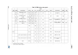


UM2
4
69
Ele
c
tric
al
sch
emat
ics
UM2
469
Re
v 1
41
/59
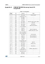
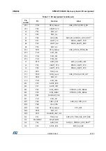
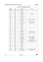
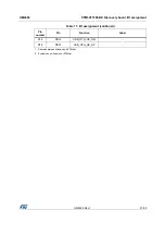
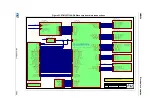
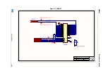
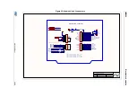
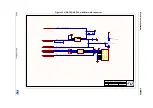
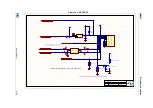
Figure 25. STM32F730I8K6 connections
3
12
STM32 MCU
MB1260
D02
11/09/2018
Title:
Size:
Reference:
Date:
Sheet:
of
A3
Revision:
STM32F723E/F7308 DISCOVERY
Project:
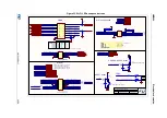
NRST
NRST
BOOT0
VDDA
VREF+
3V3
Ceramic capacitor (Low ESR)
VDDA
3V3
R50
0
R49
0
X2
NX3215SA-32.768K
VDD
4
OUT
3
EN
1
GND
2
X3
NZ2520SB-25.00M
3V3
C55
100nF
OSC_25M
C60
100nF
C38
100nF
C47
100nF
C39
100nF
C36
100nF
C52
100nF
C53
100nF
C59
100nF
C62
100nF
C46
100nF
C61
100nF
C45
100nF
C37
100nF
C40
100nF
C44
100nF
C56
100nF
3V3
USB_OTGHS_OVCR
QSPI_D0
QSPI_D3
QSPI_D2
QSPI_D1
QSPI_CLK
QSPI_NCS
SAI2_I2C1_SDA
SAI2_I2C1_SCL
SAI2_MCLK_A
SAI2_SCK_A
SAI2_FS_A
SAI2_SD_A
SAI2_SD_B
SAI2_INT
SYS_B_USER
SYS_STLINK_JTMS
SYS_STLINK_JTCK
SYS_STLINK_JTDO-SWO
VCP_RX
VCP_TX
PSRAM_A[0..17]
LCD_PSRAM_D[0..15]
LCD_PSRAM_NWE
LCD_PSRAM_NOE
PSRAM_NE1
PSRAM_NBL0
PSRAM_NBL1
ARD_A[0..5]
ARD_D[0..15]
R60
2K7
R59
2K7
2K7
R52
3V3
QSPI_D0
QSPI_D1
QSPI_D2
QSPI_D3
QSPI_NCS
QSPI_CLK
ARD_D[0..15]
SYS_B_USER
PSRAM_NBL0
PSRAM_NBL1
LCD_PSRAM_NOE
LCD_PSRAM_NWE
PSRAM_NE1
PSRAM_A[0..17]
VCP_TX
SYS_STLINK_JTCK
SYS_STLINK_JTMS
SYS_STLINK_JTDO-SWO
VCP_RX
USB_OTGHS_ID
USB_OTGHS_VBUS
USB_OTGHS_N
USB_OTGHS_OVCR
USB_OTGHS_P
VDD
VDD
VDD
VDD
VDD
VDD
C66
4.7uF
C34
4.7uF
C65
1uF
C64
1uF
C49
2.2uF
C58
2.2uF
L1
FCM1608KF-601T03
R61
10K
3V3
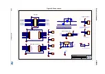
JP1
LCD_PSRAM_D[0..15]
WIFI_TX
WIFI_RX
WIFI_RST
SAI2_SD_B
SAI2_I2C1_SDA
SAI2_I2C1_SCL
SAI2_INT
SAI2_MCLK_A
SAI2_SCK_A
SAI2_FS_A
SAI2_SD_A
ARD_A[0..5]
WIFI_RST
WIFI_RX
WIFI_TX
SYS_LD_USER1
SYS_LD_USER1
SYS_LD_USER2
SYS_LD_USER2
TP14
TP15
TP7
TP11
TP12
TP4
TP6
USB_OTGHS_PPWR_EN
USB_OTGHS_PPWR_EN
USB_OTGFS_OVCR
USB_OTGFS_OVCR
USB_OTGFS_PPWR_EN
USB_OTGFS_PPWR_EN
USB_OTGFS_ID
USB_OTGFS_VBUS
USB_OTGFS_N
USB_OTGFS_P
SYS_B_USER
ARD_D10
ARD_D1
ARD_D0
ARD_A1
ARD_D13
ARD_A0
SYS_LD_USER1
CTP_SCL
USB_OTGFS_VBUS
USB_OTGFS_ID
USB_OTGFS_N
USB_OTGFS_P
SYS_STLINK_JTMS
SYS_STLINK_JTCK
STMOD+_TIM2_CH1
ARD_D5
SYS_LD_USER2
QSPI_CLK
SYS_STLINK_JTDO-SWO
ARD_D12
ARD_D11
QSPI_NCS
NC1
SAI2_I2C1_SCL
SAI2_I2C1_SDA
USB_OTGFS_OVCR
PMOD_INT
USB_OTGHS_ID
USB_OTGHS_VBUS
USB_OTGHS_N
USB_OTGHS_P
ARD_A4
ARD_A5
ARD_A2
STMOD+_SPI2_MOSIs
ARD_D2
VCP_TX
VCP_RX
LCD_TE_INT
QSPI_D0
QSPI_D1
NC11
LCD_PSRAM_D2
LCD_PSRAM_D3
WIFI_CH_PD
LCD_PSRAM_NOE
LCD_PSRAM_NWE
WIFI_GPIO_2
PSRAM_NE1
LCD_PSRAM_D13
LCD_PSRAM_D14
LCD_PSRAM_D15
PSRAM_A16
PSRAM_A17
QSPI_D3
LCD_PSRAM_D0
LCD_PSRAM_D1
PSRAM_NBL0
PSRAM_NBL1
QSPI_D2
ARD_D7
ARD_D8
ARD_D3
ARD_D6
LCD_PSRAM_D4
LCD_PSRAM_D5
LCD_PSRAM_D6
LCD_PSRAM_D7
LCD_PSRAM_D8
LCD_PSRAM_D9
LCD_PSRAM_D10
LCD_PSRAM_D12
LCD_PSRAM_D11
PSRAM_A0
PSRAM_A1
PSRAM_A2
PSRAM_A3
PSRAM_A4
PMOD_UART7_RXD
PSRAM_A5
PMOD_UART7_TXD
PMOD_UART7_RTS
PMOD_UART7_CTS
ARD_A3
PMOD_SEL_0
PSRAM_A6
PSRAM_A7
PSRAM_A8
PSRAM_A9
PSRAM_A10
PSRAM_A11
PSRAM_A12
PSRAM_A13
PSRAM_A14
PSRAM_A15
USB_OTGFS_PPWR_EN
LCD_NE
SAI2_SD_B
NC4
PMOD_GPIO_0
WIFI_GPIO_0
WIFI_RST
SAI2_INT
PMOD_GPIO_1
ARD_D4
ARD_D15
ARD_D14
ARD_D9
LCD_RST
CTP_SDA
USB_OTGHS_OVCR
CTP_RST
LCD_BL
USB_OTGHS_PPWR_EN
STMOD+_UART4_TXD
STMOD+_UART4_RXD
PMOD_RESET
PMOD_SPI2_NSS
PMOD_SPI2_SCK
PMOD_SPI2_MISO
PMOD_SPI2_MOSI
SAI2_MCLK_A
SAI2_SCK_A
SAI2_SD_A
SAI2_FS_A
NC8
CTP_INT
NC10
PC14-OSC32_IN
PC15-OSC32_OUT
REXT_OTGPHY
V12_OTGPHY
STMOD+_TIM2_CH1
PMOD_UART7_TXD
PMOD_UART7_RTS
PMOD_UART7_CTS
STMOD+_UART4_TXD
STMOD+_UART4_RXD
STMOD+_TIM2_CH1
STMOD+_UART4_RXD
PMOD_UART7_RTS
PMOD_UART7_TXD
PMOD_UART7_CTS
STMOD+_UART4_TXD
PMOD_UART7_RXD
PMOD_UART7_RXD
PMOD_RESET
PMOD_SPI2_MISO
PMOD_SPI2_MOSI
STMOD+_UART4_RXD_s
PMOD_INT
PMOD_RESET
PMOD_SPI2_MOSI
PMOD_SPI2_MISO
STMOD+_UART4_RXD_s
PMOD_INT
PMOD_SPI2_NSS
PMOD_SPI2_NSS
PMOD_SPI2_SCK
PMOD_SPI2_SCK
3V3
R44
2K7
3V3
R42
2K7
R56
2K7
TP5
TP8
LCD_BL
LCD_BL
LCD_NE
LCD_TE_INT
CTP_SCL
CTP_SDA
CTP_INT
LCD_RST
CTP_INT
LCD_RST
CTP_RST
CTP_RST
LCD_NE
LCD_TE_INT
CTP_SCL
CTP_SDA
USB_OTGHS_VBUS
USB_OTGHS_N
USB_OTGHS_P
USB_OTGHS_ID
USB_OTGFS_VBUS
USB_OTGFS_N
USB_OTGFS_P
USB_OTGFS_ID
STMOD+_SPI2_MOSIs
STMOD+_SPI2_MOSIs
TP3
PA0
PA1
PA2
PA3
PA4
PA5
PA6
PA7
PA8
PA9
PA10
PA11
PA12
PA13
PA14
PA15
PB0
PB1
PB2
PB3
PB4
PB5
PB6
PB7
PB8
PB9
PB10
PB11
PB12
PB13
PB14
PB15
PC0
PC1
PC2
PC3
PC4
PC5
PC6
PC7
PC8
PC9
PC10
PC11
PC12
PC13
PD0
PD1
PD2
PD3
PD4
PD5
PD6
PD7
PD8
PD9
PD10
PD11
PD12
PD13
PD14
PD15
PE0
PE1
PE2
PE3
PE4
PE5
PE6
PE7
PE8
PE9
PE10
PE11
PE12
PE13
PE14
PE15
PF0
PF1
PF2
PF3
PF4
PF5
PF6
PF7
PF8
PF9
PF10
PF11
PF12
PF13
PF14
PF15
PG0
PG1
PG2
PG3
PG4
PG5
PG8
PG9
PG10
PG11
PG12
PG13
PG14
PG15
PH2
PH3
PH4
PH5
PH6
PH7
PH8
PH9
PH10
PH11
PH12
PH13
PH14
PH15
PI0
PI1
PI2
PI3
PI4
PI5
PI6
PI7
PI8
PI9
PI10
PI11
PDRON
PC14
PC15
PH0
PH1
NRST
BOOT0
PDR_ON
PH0-OSCIN
PH1-OSCOUT
BYPASSREG
VCAP1
VCAP2
PMOD_SEL_1
STMOD+_UART4_RXD_s
WIFI_RX
WIFI_TX
TP13
1%
R54
3K
2.2uF
C54
10K
R36
10K
R45
10K
R55
10K
Fitted: NO
R57
10K
Fi
tt
ed
:
N
O
R43
10K
Fi
tt
ed
:
N
O
R37
0
R27
0
R62
R51
100
PMOD_GPIO_1
PMOD_GPIO_1
PMOD_GPIO_0
PMOD_GPIO_0
WIFI_GPIO_0
WIFI_GPIO_0
WIFI_GPIO_2
WIFI_GPIO_2
WIFI_CH_PD
WIFI_CH_PD
R101
0
LCD-RS_A0
LCD-RS_A0
LCD-RS_A0
PMOD_SEL_0
PMOD_SEL_0
(*)
ARD A1 conflict with STMOD+ ADC DAC (PA4)
ARD D5 conflict with STMOD+ PWM (PB0)
ARD D14 shared with STMOD+ I2C2 SDA (PH5)
ARD D15 shared with STMOD+ I2C2 SCL (PH4)
C93
100nF
Place near MCU
PMOD_SEL_0/1 => SPI2 or UART7 to PMOD#1-4
STMOD+_SPI2_MISOs
STMOD+_SPI2_MISOs
STMOD+_SPI2_MISOs
PMOD_SEL_1
PMOD_SEL_1
PMOD_SEL_0
PMOD_SEL_1
PMOD#1
PMOD#2
PMOD#3
PMOD#4
0
NSS
MOSIp
MISOp
SCK
CTS
TX
RX
RTS
NSS
SCK
TX
RX
SPI
UART
(*) default configuration to support MikroBus modules using MB1280 fan-out board
UART/SPI
0
0 (*)
1 (*)
1
1
4.7pF
C48
4.7pF
C51
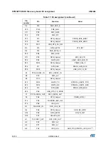
PC13-ANTI_TAMP
D1
PC0
M2
PC1
M3
PC2
M4
PC3
M5
PA0-WKUP
N3
PA1
N2
PA2
P2
PA3
R2
PA4
N4
PA5
P4
PA6
P3
PA7
R3
PC4
N5
PC5
P5
PB0
R5
PB1
R4
PB2
M6
PB10
R12
PB11
R13
PB12
P12
PB13
P13
PB14-OTG_HS_DM
R14
PB15-OTG_HS_DP
R15
PC6
H15
PC7
G15
PC8
G14
PC9
F14
PA8
F15
PA9
E15
PA10
D15
PA11
C15
PA12
B15
PA13
A15
PA14
A14
PA15
A13
PC10
B14
PC11
B13
PC12
A12
PB3
A10
PB4
A9
PB5
A6
PB6
B6
PB7
B5
PB8
A5
PB9
B4
PC14-OSC32_IN
E1
PC15-OSC32_OUT
F1
PH0-OSC_IN
G1
PH1-OSC_OUT
H1
NRST
J1
BOOT0
D6
PDR_ON
C6
OTG_HS_REXT
J15
OTG_HS_VDD12
J14
U8A
STM32F730I8K6
PE2
A2
PE3
A1
PE4
B1
PE5
B2
PE6
B3
PF0
E2
PF1
H3
PF2
H2
PF3
J2
PF4
J3
PF5
K3
PF6
K2
PF7
K1
PF8
L3
PF9
L2
PF10
L1
PH2
F4
PH3
G4
PH4
H4
PH5
J4
PF11
R6
PF12
P6
PF13
N6
PF14
R7
PF15
P7
PG0
N7
PG1
M7
PE7
R8
PE8
P8
PE9
P9
PE10
R9
PE11
P10
PE12
R10
PE13
N11
PE14
P11
PE15
R11
PH6
M11
PH7
N12
PH8
M12
PH9
M13
PH10
L13
PH11
L12
PH12
K12
PG2
L15
PG3
K15
PG4
K14
PG5
K13
PG8
H14
PH13
E12
PH14
E13
PH15
D13
PG9
C10
PG10
B10
PG11
B9
PG12
B8
PG13
A8
PG14
A7
PG15
B7
PE0
A4
PE1
A3
PD8
P15
PD9
P14
PD10
N15
PD11
N14
PD12
N13
PD13
M15
PD14
M14
PD15
L14
PD0
B12
PD1
C12
PD2
D12
PD3
D11
PD4
D10
PD5
C11
PD6
B11
PD7
A11
PI8-ANTI_TAMP2
D2
PI9
D3
PI10
E3
PI11
E4
PI0
E14
PI1
D14
PI2
C14
PI3
C13
PI4
D4
PI5
C4
PI6
C3
PI7
C2
U8B
STM32F730I8K6
VBAT
C1
VS
S
F9
VS
S
F8
VREF-
N1
VSSA
M1
VREF+
P1
VSS
H9
VSS
H10
VCAP2
F13
VSS
J6
VDD4
K4
VDD3
C5
VSS
J7
VCAP1
M10
VSS
J8
VDD2
G13
VSS
J9
VSS
J10
VDD1
N10
VDD5
G3
VDDA
R1
VDD_MMC33
C8
VDD11
C7
VDD13
F3
VDD14
J12
VDD15
C9
VSS
K6
VSS
K7
VS
S
F1
0
VS
S
G6
BYPASS-REG
L4
VDD6
N8
VDD7
N9
VDD8
J13
VDD_USB33
H13
VS
S
G7
VS
S
G8
VSS
H6
VSS
H7
VSS
H8
VSS
K8
VSS
K9
VSS
K10
VSS2
F12
VSS3
D5
VSS5
G2
VSS6
M8
VS
S
G9
VS
S
G1
0
VS
S
7
M9
VS
S
9
G1
2
VS
S
1
0
D8
VS
S
1
1
D7
VS
S
1
3
F2
VS
S
1
4
H1
2
VS
S
1
5
D9
VS
S
F6
VS
S
F7
U8C
STM32F730I8K6