background image

UM2469 Rev 1

27/59

 UM2469

Connectors

58

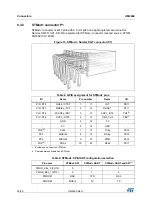
Refer to 

Section Appendix C: Pmod™ and STMod+ schematic table

 to find more 

information about STMod+ signals available on P1 connector. Refer to 

Section Appendix D: 

Fanout board

 to find more information about STMod+ compatible Fanout board.

8.4 

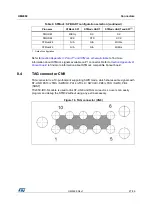
TAG connector CN9

TAG connector is a 10-pin footprint supporting SWD mode, which shares same signals with 
ST-LINK: PA13 (JTMS / SWDIO), PA14 (JTCLK / SWCLK), PB3 (JTDO / SWO), PB4 
(NRST). 

TC2050-IDC-NL cable is used to link ST-LINK and TAG connector, so users can easily 
program and debug the STM32 without using any extra accessory. 

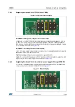
Figure 16. TAG connector (CN9)

PMOD#3

MISOp

RX

RX

PMOD#4

SCK

RTS

SCK

STMod+#8

N/A

N/A

MOSIs

STMod+#9

N/A

N/A

MISOs

1. Default configuration.

Table 9. STMod+: SPI/UART configuration selection (continued)

Pin name

STMod+ SPI

STMod+ UART

STMod+ UART and SPI

(1)

Summary of Contents for STM32F7308-DK

Page 1: ...ired for users to get started quickly and develop applications easily The full range of hardware features on the board helps users to evaluate almost all peripherals USB OTG HS and FS USART SAI Audio DAC stereo with audio jack input and output ST MEMS digital microphones external PSRAM Quad SPI Flash memory LCD with capacitive multi touch panel and others and develop applications Arduino Uno V3 Pm...

Page 2: ...15 7 4 Power supply 15 7 4 1 Supplying the board through the ST LINK USB port default setting 15 7 4 2 Supplying the board through a charger connected to ST LINK 16 7 4 3 Supplying the board from E5V CN3 or CN12 17 7 4 4 Supplying the board from an external power supply through USB HS 17 7 4 5 Supplying the board from an external power supply through USB FS 18 7 5 Programming debugging when the po...

Page 3: ...Frida connector 30 8 9 ST LINK V2 1 USB Micro B connector CN1 31 8 10 Audio stereo speakers 31 8 11 Audio line connectors 31 8 11 1 Audio line output green jack connector 32 8 11 2 Audio line input blue jack connector 32 Appendix A STM32F7308 DK Discovery board I O assignment 33 Appendix B Electrical schematics 38 Appendix C Pmod and STMod schematic table 51 Appendix D Fanout board 53 D 1 MikroEle...

Page 4: ... Industry Canada IC Compliance Statements 56 E 1 FCC Compliance Statement 56 E 1 1 Part 15 19 56 E 1 2 Part 15 105 56 E 1 3 Part 15 21 56 E 2 IC Compliance Statement 56 E 2 1 Compliance Statement 56 E 3 Déclaration de conformité 56 Appendix F CISPR32 57 F 1 Warning 57 Revision history 58 ...

Page 5: ...AB connector CN19 28 Table 11 USB OTG FS Micro AB connector CN18 front view 28 Table 12 Pin description of the LCD Frida connector CN17 29 Table 13 Pin description of the CTP connector CN16 30 Table 14 USB Micro B connector CN1 31 Table 15 Audio line output connector CN5 32 Table 16 Audio line input connector CN4 32 Table 17 I O assignment 33 Table 18 STMod connector signals 52 Table 19 Descriptio...

Page 6: ... CN19 front view 28 Figure 18 USB OTG FS Micro AB connector CN18 front view 28 Figure 19 LCD Frida connector Hirose FH26 29S 0 3SHW CN17 front view 29 Figure 20 CTP connector Hirose DF37NB 10DS 0 4V 5x CN16 front view 30 Figure 21 USB Micro B connector CN1 front view 31 Figure 22 Mechanical drawing of the audio line connector 31 Figure 23 STM32F7308 DK Discovery board interconnections 39 Figure 24...

Page 7: ...od STMod On board ST LINK V2 1 supporting USB re enumeration capability mass storage Virtual COM port debug port Flexible power supply options ST LINK USB VBUS or external sources Power supply output for external applications 3 3 V or 5 V Fanout board included inside the board package compatible with MikroElektronika Click boards ESP 01 and Seeed Studio Grove modules Provision for headers for dire...

Page 8: ...o the evaluation tool ordering part number that is stuck or silkscreen printed on the board This board features a specific STM32 device version which allows the operation of any bundled commercial stack library available This STM32 device shows a U marking option at the end of the standard part number and is not available for sales In order to use the same commercial stack in his application a dev...

Page 9: ...y demonstration of the device peripherals in standalone mode The latest versions of the demonstration source code and associated documentation can be downloaded from the www st com en evaluation tools stm32f7308 dk html webpage 6 Ordering information To order the STM32F7308 DK Discovery kit refer to Table 1 Table 1 Ordering Information Order Code Target STM32 STM32F7308 DK STM32F730I8K6 ...

Page 10: ... locate these features on the STM32F7308 DK board The mechanical dimensions of the STM32F7308 DK board are showed in Figure 6 Figure 3 Hardware block diagram 1 Dotted lines identify the shared signals 06Y 9 9 3RZHU 6XSSO SXVK EXWWRQ DQG ZDNH XS 0LFUR 86 FRQQHFWRU 0LFUR 86 FRQQHFWRU L L PRGXOH FRQQHFWRU 3 2V 27 6 27 6 8 57 9 3 8 57 6 3 2V 3 2V 3 2V 3 2V 0 DGGUHVV 0 GDWD 3 2V 6 57 6 463 XGLR RGHF 3P...

Page 11: ... layout 670 RXU 67 0 06 PLFURSKRQHV RQ 6 0 LQSXWV 7 7 SL HOV 8VHU V GLVSOD FRQQHFWRU 86 27 6 0LFUR FRQQHFWRU 86 27 6 2YHU FXUUHQW 86 27 6 9 86 86 27 6 0LFUR FRQQHFWRU 302 FRQQHFWRU RQWURO 7RXFK 3DQHO FRQQHFWRU UGXLQR V L L PRGXOH FRQQHFWRU 86 27 6 9 86 86 27 6 2YHU FXUUHQW 5 6 7 EXWWRQ 83 EXWWRQ 670RG FRQQHFWRU 86 27 6 86 27 6 06Y 9 ...

Page 12: ...7 1 9 ZLWK 0LFUR FRQQHFWRU 7 GHEXJ FRQQHFWRU 670 0 8 9 SRZHU VHOHFWLRQ UGXLQR 812 9 FRQQHFWRUV 670 7 IRU 67 1 0ELW 365 0 PHPRU 6WHUHR VSHDNHU RXWSXWV XGLR RGHF 670 QSXW XGLR OLQH MDFN 2XWSXW XGLR OLQH MDFN 67 1 20 9 32 5 67 5 3RZHU OLPLWHU IDXOW 7 9 H WHUQDO SRZHU FRQQHFWRU 0ELW 4XDG 63 ODVK PHPRU 06Y 9 ...

Page 13: ...re layout and configuration 58 7 2 The STM32F7308 DK Discovery kit mechanical drawing Figure 6 STM32F7308 DK mechanical drawing 1 The digital microphones marked in orange U16 U17 U18 and U19 are placed on the bottom side of the board ...

Page 14: ...common to both versions V2 and V2 1 refer to the ST LINK V2 in circuit debugger programmer for STM8 and STM32 user manual UM1075 7 3 1 Drivers Before connecting the STM32F7308 DK board to a Windows 7 Windows 8 or Windows 10 PC via USB a driver for ST LINK V2 1 must be installed It can be downloaded from the www st com website In case the STM32F7308 DK board is connected to the PC before installing...

Page 15: ...NK USB port through a USB Type A to Micro B cable 5 V DC power is provided by VBUS from the USB type Micro B connector CN1 of ST LINK V2 1 USB 5 V power source on silkscreen ST LINK see Figure 8 If the USB enumeration succeeds as explained below the ST LINK 5 V link power is enabled by asserting the PWR_ENn signal This pin is connected to U1 a power switch ST890 which powers the board This power s...

Page 16: ...n this specific case the resistor R5 needs to be soldered to allow the board to be powered anyway The LED LD2 is lit when the STM32F7308 DK board is powered by the 5 V correctly Caution Do not connect a PC to ST LINK CN1 when R5 is soldered The PC may be damaged or the board not powered correctly 7 4 2 Supplying the board through a charger connected to ST LINK The 5 V DC power charger is connected...

Page 17: ...on silkscreen E5V see Figure 10 From E5V 7 12V DC power from CN12 VIN 7 12 V DC power supply is provided by an Arduino Uno V3 compatible shield connected to CN11 CN12 CN13 and CN15 connectors This 7 12 V voltage VIN is then converted to 5 V by a LDO U11 Finally the user must fit the jumper on E5V position on CN8 connector to select this LDO output E5V as main power supply for the board see Figure ...

Page 18: ...d 1 Connect the jumper CN8 on E5V or USB_HS or USB_FS 2 Connect the external power source to CN3 or CN12 or CN18 or CN19 3 Check that the red LED LD2 is turned ON 4 Connect the PC to USB connector CN1 If this order is not respected the STM32F7308 DK Discovery board may be powered by VBUS first from ST LINK and the following risks may be encountered 1 If more than 500 mA current is needed by the bo...

Page 19: ...is connected to SAI interface of STM32F730I8K6 It communicates with STM32F730I8K6 via I2 C bus The analog line input is connected to ADC of WM8994ECS R through blue audio jack CN4 The analog line output is connected to DAC of WM8994ECS R via green audio jack CN5 Two external speakers can be connected to WM8994ECS R via CN10 for left speaker and CN7 for right speaker Four digital microphones ST MEM...

Page 20: ...wered by an external power supply through USB HS connector CN19 in device mode do not use a PC as power source see Section 7 4 4 7 10 USB OTG FS The STM32F7308 DK board supports USB OTG full speed communication via a USB Micro AB connector A USB power switch is also connected on VBUS and provides power to CN18 The green LED LD9 is lit in one of these cases Power switch is ON and the STM32F7308 DK ...

Page 21: ...N1 The virtual COM port settings are configured as 115200 b s 8 bits data no parity 1 stop bit no flow control 7 14 TFT LCD 240x240 pixels A 240x240 pixel TFT LCD FRD154BP2902 from Frida is connected to FMC data interface of STM32F730I8K6 It uses the Sitronix ST7789H2 controller for 262K color TFT LCD graphic type Display data are stored in the on chip display data RAM of 240x320x18 bits It perfor...

Page 22: ...ser The LEDs are LD1 Arduino blue LD5 User 1 red and LD6 User 2 green To light a LED a low logic state 0 should be written in the corresponding GPIO Table 3 gives the assignment of control ports to the LED indicators Table 3 Control port assignment Reference Color Name Comment B1 BLUE USER Alternate function Wake up B2 BLACK RESET LD1 BLUE ARDUINO PA5 LD2 RED 5 V Power LD3 RED Fault Power Current ...

Page 23: ...ible with Arduino Uno V3 standard Most shields designed for Arduino Uno V3 are also supported by the STM32F7308 DK board The Arduino connectors on STM32F7308 DK board support the Arduino Uno V3 Caution The I Os of STM32 microcontroller are 3 3 V compatible instead of 5 V for Arduino Uno V3 Table 4 Wi Fi extension connector CN14 Pin number Wi Fi description 1 WIFI_RX 2 3 3 V 3 GPIO0 4 WIFI RST 5 GP...

Page 24: ...mpatible Fanout board The user must select the different configurations using PMOD_SEL_0 PH15 and PMOD_SEL_1 PI10 to control the STG3692QTR U20 This quad analog S P D T Single Pole Dual Throw allows to connect Pmod and STMod either to UART or to SPI or to both in case of STMod Table 5 GPIO assignment for Arduino pins I O Name Pin number Name I O CN11 10 SCL2 PH4 1 1 Shared between Arduino and STMo...

Page 25: ...ection Appendix C Pmod and STMod schematic table to find more information about Pmod pins Table 6 GPIO assignment for Pmod pins I O Name Pin number Name I O PI0 PF9 NSS2 CTS7 1 7 INT PB11 PI3 PF7 MOSI2p TX7 2 8 RESET PF11 PI2 PF6 MISO2p RX7 3 9 GPIO0 PG12 PI1 PF8 SCK2 RTS7 4 10 GPIO1 PH2 GND 5 11 GND 3 3 V 6 12 3 3 V Table 7 Pmod SPI or UART configuration selection Pin name Pmod SPI Pmod UART PMOD...

Page 26: ...r Name I O PI0 PF9 NSS2 CTS7 1 11 INT PB11 PI3 PF7 MOSI2p TX7 2 12 RESET PF11 PI2 PF6 MISO2p RX7 3 13 ADC1_IN14 PC4 1 1 Exclusive use Arduino or STMod PI1 PF8 SCK2 RTS7 4 14 TIM3_CH3 PB0 1 GND 5 15 5 V 5 V 6 16 GND PH4 2 2 Shared between Arduino and STMod SCL2 7 17 TX4p PH13 PC3 MOSI2s 8 18 RX4p PH14 PC2 MISO2s 9 19 PWM PA15 PH5 2 SDA2 10 20 RX4s PC11 Table 9 STMod SPI UART configuration selection...

Page 27: ...0 pin footprint supporting SWD mode which shares same signals with ST LINK PA13 JTMS SWDIO PA14 JTCLK SWCLK PB3 JTDO SWO PB4 NRST TC2050 IDC NL cable is used to link ST LINK and TAG connector so users can easily program and debug the STM32 without using any extra accessory Figure 16 TAG connector CN9 PMOD 3 MISOp RX RX PMOD 4 SCK RTS SCK STMod 8 N A N A MOSIs STMod 9 N A N A MISOs 1 Default config...

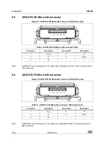
Page 28: ... 6 USB OTG FS Micro AB connector Figure 18 USB OTG FS Micro AB connector CN18 front view Note STMPS U14 is providing VBUS It is active low controlled by PG8 Overcurrent is sent to PB10 interrupt Table 10 USB OTG HS Micro AB connector CN19 Pin number Description Pin number Description 1 VBUS 4 ID 2 D 5 GND 3 D Table 11 USB OTG FS Micro AB connector CN18 front view Pin number Description Pin number ...

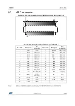
Page 29: ...cription Pin connection Pin number Description Pin connection 1 GND GND 2 FMARK PC8 TE INT 3 DB15 FMC_D15 4 DB14 FMC_D14 5 DB13 FMC_D13 6 DB12 FMC_D12 7 DB11 FMC_D11 8 DB10 FMC_D10 9 DB9 FMC_D9 10 DB8 FMC_D8 11 DB7 FMC_D7 12 DB6 FMC_D6 13 DB5 FMC_D5 14 DB4 FMC_D4 15 DB3 FMC_D3 16 DB2 FMC_D2 17 DB1 FMC_D1 18 DB0 FMC_D0 19 NRD FMC_NOE 20 NWR FMC_NWE 21 RS PF0 FMC_A0 22 NCS PG9 NE 23 RESET PH7 LCD_RS...

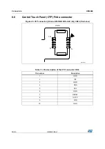
Page 30: ...ol Touch Panel CTP Frida connector Figure 20 CTP connector Hirose DF37NB 10DS 0 4V 5x CN16 front view Table 13 Pin description of the CTP connector CN16 Pin number Description 1 GND 2 INT 3 GND 4 SDA 5 SCL 6 GND 7 RESET 8 IOVCC 9 VDD 10 GND 06Y 9 1 ...

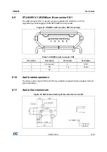
Page 31: ...microcontroller Figure 21 USB Micro B connector CN1 front view 8 10 Audio stereo speakers The stereo audio outputs CN10 and CN7 are available to support stereo speakers left and right respectively 8 11 Audio line connectors Figure 22 Mechanical drawing of the audio line connector Table 14 USB Micro B connector CN1 Pin number Description Pin number Description 1 VBUS power 4 GND 2 DM 5 6 Shield 3 D...

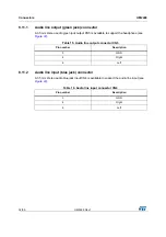
Page 32: ...pport the headphone see Figure 22 8 11 2 Audio line input blue jack connector A 3 5 mm stereo audio blue jack input CN4 is available to support the audio line input see Figure 22 Table 15 Audio line output connector CN5 Pin number Description 3 GND 4 Right 6 Left Table 16 Audio line input connector CN4 Pin number Description 3 GND 4 Right 6 Left ...

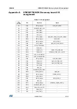
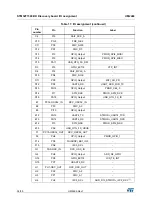
Page 33: ... A9 PB4 SPI1_MISO ARD_D12_SPI1_MISO A10 PB3 SYS_JTDO SWO A11 PD7 FMC_NE1 A12 PC12 UART5_TX UART_TXD_WIFI_RX A13 PA15 TIM2_CH1 STMOD _TIM2_CH1_2_ETR A14 PA14 SYS_JTCK SWCLK A15 PA13 SYS_JTMS SWDIO B1 PE4 GPIO_Output ARD_D8_GPIO B2 PE5 TIM9_CH1 ARD_D3_TIM9_CH1 B3 PE6 TIM9_CH2 ARD_D6_TIM9_CH2 B4 PB9 I2C1_SDA B5 PB7 FMC_NL B6 PB6 QUADSPI_BK1_NCS B7 PG15 GPIO_EXTI15 SAI2_INT B8 PG12 GPIO_Output PMOD_GP...

Page 34: ...PMOD_SPI2_SCK D15 PA10 GPIO_Output USB_OTG_FS_ID E1 PC14 OSC32_IN RCC_OSC32_IN E2 PF0 FMC_A0 E3 PI10 GPIO_Output E12 PH13 UART4_TX STMOD _UART4_TXD E13 PH14 UART4_RX STMOD _UART4_RXD E14 PI0 SPI2_NSS PMOD_SPI2_NSS E15 PA9 USB_OTG_FS_VBUS F1 PC15 OSC32_OUT RCC_OSC32_OUT F4 PH2 GPIO_Output PMOD_GPIO_1 F14 PC9 QUADSPI_BK1_IO0 F15 PA8 I2C3_SCL G1 PH0 OSC_IN RCC_OSC_IN G4 PH3 GPIO_Output ARD_D4_GPIO G1...

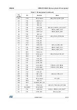
Page 35: ...9 UART7_CTS PMOD_UART7_CTS L3 PF8 UART7_RTS PMOD_UART7_RTS L12 PH11 TIM5_CH2 L13 PH10 GPIO_Input USB_OTGHS_OVCR_INT L14 PD15 FMC_D1 L15 PG2 FMC_A12 M2 PC0 ADC2_IN10 M3 PC1 ADC2_IN11 M4 PC2 SPI2_MISO STMOD _SPI2_MISOs M5 PC3 SPI2_MOSI STMOD _SPI2_MOSIs M6 PB2 QUADSPI_CLK M7 PG1 FMC_A11 M11 PH6 TIM12_CH1 ARD_D9_TIM12_CH1 M12 PH8 I2C3_SDA M13 PH9 GPIO_Output CTP_RST M14 PD14 FMC_D0 M15 PD13 QUADSPI_B...

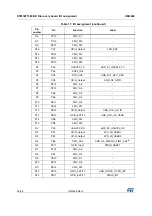
Page 36: ...8 PE8 FMC_D5 P9 PE9 FMC_D6 P10 PE11 FMC_D8 P11 PE14 FMC_D11 P12 PB12 GPIO_Output USB_OTG_HS_ID P13 PB13 GPIO_EXTI13 USB_OTG_HS_VBUS P14 PD9 FMC_D14 P15 PD8 FMC_D13 R2 PA3 USART2_RX ARD_D0_USART2_RX R3 PA7 GPIO_Output SYS_LD_USER1 R4 PB1 GPIO_Output SYS_LD_USER2 R5 PB0 TIM3_CH3 ARD_D5_STMOD _TIM3_CH3 2 R6 PF11 GPIO_Input PMOD_RESET R7 PF14 FMC_A8 R8 PE7 FMC_D4 R9 PE10 FMC_D7 R10 PE12 FMC_D9 R11 PE1...

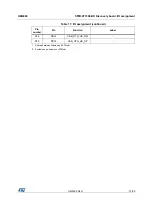
Page 37: ... STM32F7308 DK Discovery board I O assignment 58 R14 PB14 USB_OTG_HS_DM R15 PB15 USB_OTG_HS_DP 1 Shared between Arduino and STMod 2 Exclusive use Arduino or STMod Table 17 I O assignment continued Pin number Pin Function Label ...

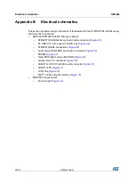
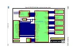
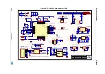
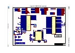
Page 38: ...DK Discovery board interconnections Figure 23 ST LINK V2 1 with support of SWD only Figure 24 STM32F730I8K6 connections Figure 25 Audio codec WOLFSON and Audio connectors Figure 26 PSRAM Figure 27 Quad SPI Flash memory MICRON Figure 28 Arduino Uno V3 connectors Figure 29 USB OTG HS PHY with Micro AB connector Figure 30 USB OTG FS Figure 31 LCD Frida Figure 32 Wi Fi LEDs and push buttons Figure 33 ...

Page 39: ... PSRAM_NE1 PSRAM_NBL0 PSRAM_NBL1 QSPI_D2 ARD_D 0 15 SAI2_SCK_A SAI2_FS_A SAI2_SD_A SAI2_SD_B SAI2_INT LCD_NE LCD_TE_INT LCD_BL LCD_RST CTP_INT CTP_RST WIFI_RST WIFI_RX WIFI_TX ARD_A 0 5 LCD_PSRAM_NOE SYS_STLINK_JTMS SYS_STLINK_JTCK SYS_STLINK_JTDO SWO VCP_RX VCP_TX USB_OTGHS_OVCR USB_OTGHS_PPWR_EN USB_OTGHS_VBUS USB_OTGHS_N USB_OTGHS_ID USB_OTGHS_P USB_OTGFS_OVCR USB_OTGFS_PPWR_EN USB_OTGFS_VBUS U...

Page 40: ...FAULT 8 U1 ST890CDR R20 10K C5 100nF 4K7 R6 R17 10K 100K R3 100K Fitted NO R24 R23 100 T_SWO R13 330 R14 330 1 8 Volts Output SB7 SB12 SB11 SB10 SB3 3V3 E5V Arduino UNO power pin VIN Vin 3 Vout 2 Gnd 1 Tab 4 U11 LD1117S50TR E5V 1 2 X1 NX3225GD 8 00M MCO Ilim 625mA 1 2Ilim 750mA Isc 1 5Ilim 938mA Isc 0 Fitted NO R5 Must be on a border or the PCB 5V_USB_HS T_JTDO T_JTDI T_JRST 1V8 3V3 Vin 3 Vout 2 G...

Page 41: ..._UART4_RXD_s PMOD_INT PMOD_SPI2_NSS PMOD_SPI2_NSS PMOD_SPI2_SCK PMOD_SPI2_SCK 3V3 R44 2K7 3V3 R42 2K7 R56 2K7 TP5 TP8 LCD_BL LCD_BL LCD_NE LCD_TE_INT CTP_SCL CTP_SDA CTP_INT LCD_RST CTP_INT LCD_RST CTP_RST CTP_RST LCD_NE LCD_TE_INT CTP_SCL CTP_SDA USB_OTGHS_VBUS USB_OTGHS_N USB_OTGHS_P USB_OTGHS_ID USB_OTGFS_VBUS USB_OTGFS_N USB_OTGFS_P USB_OTGFS_ID STMOD _SPI2_MOSIs STMOD _SPI2_MOSIs TP3 PA0 PA1 ...

Page 42: ...2 C1 SPKMODE A3 SPKOUTLN B1 SPKOUTLP A2 SPKOUTRN C3 SPKOUTRP B3 SPKVDD1 B2 SPKVDD2 C2 VMIDC C9 VREFC E6 U7 WM8994ECS R 1V8 3V3 3V3 3V3 MIC_VDD1 Bottom Left Top Left GND 5 LR 2 CLK 3 VDD 1 DOUT 4 U16 MP34DT01 GND 5 LR 2 CLK 3 VDD 1 DOUT 4 U18 MP34DT01 SPK Left SPK Right Right Left Jack Line output Green Jack Line input blue Right Left C22 4 7uF R46 10K R85 10K C19 4 7uF C31 4 7uF R35 0 C33 100nF C4...

Page 43: ...A16 PSRAM_A17 PSRAM_A 0 17 LCD_PSRAM_D 0 15 LCD_PSRAM_NWE LCD_PSRAM_NOE PSRAM_NE1 PSRAM_NBL0 PSRAM_NBL1 PSRAM_NBL0 PSRAM_NBL1 LCD_PSRAM_NOE LCD_PSRAM_NWE i PSRAM_A Matched Net Lengths Tolerance 200mil Impedance Constraint Min 40 00 Max 60 00 i PSRAM_D Matched Net Lengths Tolerance 200mil Impedance Constraint Min 40 00 Max 60 00 i PSRAM_A i PSRAM_A i PSRAM_A i PSRAM_A 10K R63 0 R65 0 R64 PSRAM Data...

Page 44: ...I_D0 QSPI_D1 QSPI_D2 QSPI_D3 QSPI_NCS QSPI_CLK DQ3 HOLD 7 VCC 8 S 1 DQ1 2 C 6 DQ0 5 VSS 4 DQ2 Vpp W 3 DQ3 HOLD VCC S DQ1 C DQ0 VSS DQ2 Vpp W Fitted NO U6 N25Q512A13GF840E MICRON i QSPI i QSPI i QSPI i QSPI i QSPI i QSPI Matched Net Lengths Tolerance 100mil 100nF C13 10K R30 2nd source not footprint compatible SIO3 RESET 7 VCC 8 CS 1 SIO1 SO 2 SCLK 6 SIO0 SI 5 GND 4 SIO2 WP 3 SIO3 RESET VCC CS SIO1...

Page 45: ...MOSI SPI1_MISO SPI1_SCK IOREF NRST 3V3 5V GND GND VIN POWER AIN TIM9_CH2 SB14 3V3 5V PH4 PH5 PH4 PH5 ARD_A 0 5 ARD_D 0 15 ARD_A 0 5 ARD_D 0 15 ARD_A0 ARD_D0 ARD_D1 ARD_D2 ARD_D3 ARD_D4 ARD_D5 ARD_D6 ARD_D7 ARD_D8 ARD_D9 ARD_D10 ARD_D11 ARD_D12 ARD_D13 ARD_D14 ARD_D15 ARD_D14 ARD_D15 ARD_A1 ARD_A2 ARD_A3 SDA D14 SCL D15 PA3 R53 0 SB36 SB38 ARD_A4 ARD_A5 ADC1_IN10 ADC1_IN11 PC0 PC1 1 2 3 4 5 6 CN15 ...

Page 46: ...TGHS_P 3 1 2 T1 9013 SOT23 GND 2 IN 5 EN 4 OUT 1 FAULT 3 U13 STMPS2151STR LD8 LED green LD7 LED red R78 0 5V_USB_HS R80 3K3 100K R75 USB_OTGHS_VBUS USB_OTGHS_ID USB_OTGHS_OVCR USB_OTGHS_PPWR_EN USB_OTGHS_OVCR USB_OTGHS_VBUS USB_OTGHS_N USB_OTGHS_P USB_OTGHS_ID USB_OTGHS_PPWR_EN ID 4 Gnd 8 Gnd 5 Vbus 1 D in 7 D out 2 D in 6 D out 3 U15 ECMF02 4CMX8 USB_OTGHS_CN_N USB_OTGHS_CN_P i USB Matched Net Le...

Page 47: ...B_OTGFS_ID USB_OTGFS_OVCR i USB Matched Net Lengths Tolerance 0 2mm Impedance Constraint Min 85 00 Max 95 00 i USB i USB i USB 47K R73 0 R72 47K R79 620 R84 0 R99 LD10 LED red VBUS 1 DM 2 DP 3 ID 4 GND 5 Shield 6 USB_Micro AB receptacle Shield 7 Shield 8 Shield 9 EXP 10 CN18 475900001 47K R77 GND 2 IN 5 EN 4 OUT 1 FAULT 3 U14 STMPS2141STR LD9 LED green 3 1 2 T2 9013 SOT23 10K R76 330 R83 C77 4 7uF...

Page 48: ...D_PSRAM_D11 LCD_PSRAM_D12 LCD_PSRAM_D13 LCD_PSRAM_D14 LCD_PSRAM_D15 LCD_BL Backlight control ON OFF or dimmer by low frequency 1 to 10kHz typ PWM using TIM5_CH2 LCD_BL LCD_BL LCD_PSRAM_D 0 15 LCD_NE LCD RS_A0 LCD_PSRAM_NWE LCD_PSRAM_NOE LCD_TE_INT CTP_SCL CTP_SDA CTP_INT LCD_RST CTP_INT LCD_RST CTP_RST CTP_RST CTP_INT CTP_RST LCD_PSRAM_D 0 15 LCD_NE LCD RS_A0 LCD_PSRAM_NWE LCD_PSRAM_NOE LCD_TE_INT...

Page 49: ...MOSI PMOD_SPI2_NSS PMOD_SPI2_MISO PMOD_UART7_RXD PMOD_UART7_RTS PMOD_UART7_CTS PMOD_UART7_TXD PMOD_SPI2_SCK 1 2 3 4 5 6 7 8 9 10 11 12 13 14 15 16 17 18 19 20 P1 SQT 110 01 F D RA 10K Fitted NO R91 PMOD_GPIO_1 PMOD_GPIO_0 R93 10K R96 10K 3V3 WIFI_GPIO_2 WIFI_GPIO_0 R95 10K WIFI_CH_PD 5V WIFI_GPIO_0 WIFI_GPIO_0 WIFI_GPIO_2 WIFI_GPIO_2 WIFI_CH_PD WIFI_CH_PD PC12 PG13 PD6 PG14 PD3 PD2 PA0 PA7 PB1 1 2...

Page 50: ...OD 4 PMOD 7 PMOD 8 PMOD 9 PMOD 10 PMOD 11 PMOD 12 PMOD 13 PMOD 14 PMOD 17 PMOD 18 PMOD 19 PMOD 20 PMOD 11 PMOD 12 PMOD 13 PMOD 14 PMOD 3 PMOD 2 PMOD 11 PMOD 14 PMOD 12 PMOD 13 PMOD 7 PMOD 10 I2C_SCL I2C_SDA VCC 5V 5V 3V3 PMOD 1 NSS CTS PMOD 2 MOSIp TX PMOD 3 MISOp RX PMOD 4 SCK RTS PMOD 7 SCL PMOD 8 MOSIs PMOD 9 MISOs PMOD 10 SDA AN RST CS SCK MISO MOSI 3 3V GND PWM INT RX TX SCL SDA 5V GND GND GP...

Page 51: ...r Arduino Uno V3 A switch controlled by software is present to select which function is used using PI10 and PH15 PIOs Analog signals are in brackets xxx The I2 C bus is shared with the Arduino Uno V3 connectors It is recommended to check the device slave address when adding it to the bus Refer to the following list of acronyms before reading the Table 18 RTS7 stands for USART7_RTS ADC2 4 stands fo...

Page 52: ...15 1 PF6 3 13 PA4 ADC DAC 1 NSS1 NSS3 CK2 ADC2 4 DACOUT1 1 GPIO PG12 ADC 1 MISO T8 4 MISO2p PH15 0 PI2 RTS MISO5 ADC3 6 T13 1 RTS7 PI10 1 PF8 4 14 PB0 PWM 1 CTS4 ADC1 8 ADC2 8 T1 2N T3 3 T8 2N GPIO PH2 PWM 1 SCK T8 BKIN2 SCK2 PI10 0 PI1 GND GND 5 15 5 V 5 V 5 V 5 V 6 16 GND GND SCL2 2 SCL2 2 PH4 7 17 PH13 GPIO TX4 TXCAN1 T8 1N ADC1 13 ADC2 13 ADC3 13 MOSI2s PC3 8 18 PH14 GPIO RX4 RXCAN1 T8 2N ADC1...

Page 53: ...ka Click board compatible connectors CN10 and CN11 two 1x8 pin female connectors ESP 01 compatible connector CN4 2x4 pin female connector Seeed Studio Grove compatible connectors CN3 and CN2 two 1x4 pin male connectors Reserved standard 2 54 mm pitch of STMod pin header for breadboard The main active component for this Fanout board is the 3 3 V regulator U1 200 mA Figure 35 STMod Fanout module plu...

Page 54: ...onnector pins STMod connector CN11 number Function of mikroBUS Pin number Pin number Function of mikroBUS STMod connector CN10 number STMod 13 ADC 1 1 Exclusive use Arduino or STMod AN 1 1 PWM STMod 14 PWM 1 STMod 12 RST RST 2 2 INT STMod 11 INT STMod 1 NSS CS 3 3 RX STMod 3 RX STMod 4 SCK SCK 4 4 TX STMod 2 TX STMod 9 MISOs MISO 5 5 SCL STMod 7 SCL 2 2 Shared with Arduino STMod 8 MOSIs MOSI 6 6 S...

Page 55: ... connection Table 21 shows the definition of the pins D 3 2 Compatible connector for UART Grove boards Fanout CN2 The CN2 connector is compatible with Grove NFC boards using cable for connection Table 22 shows the definition of the pins Table 21 Description of the I2 C Grove board connector pins CN3 STMod connector Function of Grove CN3 PIN number STMod 7 SCL SCL 1 STMod 10 SDA SDA 2 5 V VCC 3 GND...

Page 56: ...asonable protection against harmful interference when the equipment is operated in a commercial environment This equipment generates uses and can radiate radio frequency energy and if not installed and used in accordance with the instruction manual may cause harmful interference to radio communications Operation of this equipment in a residential area is likely to cause harmful interference in whi...

Page 57: ...UM2469 Rev 1 57 59 UM2469 CISPR32 58 Appendix F CISPR32 F 1 Warning Warning This device is compliant with Class A of CISPR32 In a residential environment this equipment may cause radio interference ...

Page 58: ...Revision history UM2469 58 59 UM2469 Rev 1 Revision history Table 23 Document revision history Date Revision Changes 18 Oct 2018 1 Initial release ...

Page 59: ...sers are solely responsible for the choice selection and use of ST products and ST assumes no liability for application assistance or the design of Purchasers products No license express or implied to any intellectual property right is granted by ST herein Resale of ST products with provisions different from the information set forth herein shall void any warranty granted by ST for such product ST...

Reviews: