background image

Ov
e

rvi

ew

8

g

POWER LED

Flashes or lights based on the internal status of the 
camera.

Flashing: Obtaining IP address.
Lit: IP address obtained.

Using a Tripod

To use the tripod, install the tripod adaptor VCT-ST70I 
(not supplied) on the camera module.
Use a tripod screw with a protrusion (

4

) extending from 

the installation surface, as follows, and tighten it, using 
a screwdriver.

4.5 to 5.5 mm
0.18 to 0.22 inches

Note

If you install a tripod adapter (not supplied), use the 
screws provided.

Connecting the Cables

Connect the camera cable to the DC IN connector and 
the LAN cable to the RJ45 connector respectively. When 
you connect the LAN cable, turn the two fastening 
screws on the connector to secure the cable tightly.

a

DC IN connector

b

RJ45 connector

c

Camera cable

d

LAN cable

e

Fastening screws

Connect the other end of the camera cable to the 
DC-700/700CE and the other end of the LAN cable to 
the Network card.

Multi-Function Output 
Specifications

When exposure output is selected, signal output is valid 
during image sensor exposure. When strobe control 
output is selected, output signal timing and pulse width 
can be precisely set to control external devices such as 
strobes connected to the camera. Output signal polarity 
can be set for both exposure and strobe control outputs. 
TTL output termination impedance should be at least 
10 k

Ω


.

Illustrations of positive-polarity multi-function TTL 
output.

When using ISO (+ or -), be sure to use an external 
power supply b5 and +24 Vdc in combination 
with resistance.
Refer to the following circuit diagram.

Note

When GPO (fixed-value, general-purpose output) is 
selected, the fixed output varies depending on the 
register setting value.
Register setting value 0: fixed Low
Register setting value 1: fixed Hi

Exposure Time

Strobe control pulse width setting (time)

Strobe control signal rise time and 
pulse width are settable

4.8 to 5.2 V

0 to 4 ms

0 to 4 ms

Multi-
function 
output
3.3 V

TLP281

220 

Ω

ISO (+) [#6]

ISO (–) [#5]

470 

Ω

Summary of Contents for XCG-5005E

Page 1: ...Technical Manual A DBK 100 11 1 Digital Video Camera Module 2009 Sony Corporation XCG V60E XCG SX97E XCG U100E XCG 5005E ...

Page 2: ...igital Clamp XCG 5005E only 14 Digital Gain 14 Digital ON OFF XCG 5005E only 14 Look Up Table 14 Switching Output Bit Length 14 Test Chart 14 Partial Scan 15 Binning Mode 15 Frame Rate Control 16 Image Acquisition Modes 16 Memory Channels and User Memories 16 Network Functions 16 Control Operations Camera Control Registers 18 Camera Initialization Register 18 Image Control Registers 18 Network Con...

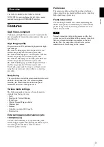
Page 3: ...ane Installing the camera module on the front panel minimizes deviation of the optical axis Various mode settings The following mode settings can be configured via controls from the host device Gain Read mode Normal Binning Partial scan Shutter Normal Trigger shutter Shutter speed Gamma Switching an output Bit Length Binarization External trigger shutter function 2 to 1 100 000 sec You can obtain ...

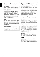
Page 4: ...e induced by infrared radiation deep in the photosensor It appears as a vertical smear since the CCD imaging element uses an interline transfer system Vertical aliasing When you shoot vertical stripes or lines they may appear jagged Blemishes A CCD image sensor consists of an array of individual sensor elements pixels A malfunctioning sensor element will cause a single pixel blemish in the picture...

Page 5: ... 32 8 ft 25N 25 m 82 ft camera cable C mount lens High resolution lens DC 700 700CE camera adaptor VCT ST70I tripod adaptor Network card commercially available LAN cable commercially available This is a small size high resolution video camera module using a progressive scan CCD image sensor This is attached to the DC IN connector of the camera module and is used for power supply and exchange of tr...

Page 6: ...XC 12P10N CCXC 12P25N Camera adaptor DC 700 700CE AC TRIG LAN cable Network card XCG V60E XCG SX97E XCG U100E XCG 5005E About multi function output You can select from the following signals based on settings Exposure output strobe control outputs fixed value Hi or Low Multi function output GPI input ...

Page 7: ...ize of the Guide hole and the Reference hole Rear e DC IN DC power input connector 12 pin You can connect a camera cable CCXC 12P05N etc to input the 12 V DC power supply The pin configuration of this connector is as follows For details on the pin arrangement see the following table About multi function output You can select from the following signals based on settings Exposure output strobe contr...

Page 8: ... the LAN cable to the Network card Multi Function Output Specifications When exposure output is selected signal output is valid during image sensor exposure When strobe control output is selected output signal timing and pulse width can be precisely set to control external devices such as strobes connected to the camera Output signal polarity can be set for both exposure and strobe control outputs...

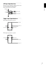
Page 9: ...h resistance Refer to the following circuit diagram Trigger Input Specifications When trigger input polarity is positive When trigger input polarity is negative GPI TLP281 470 Ω ISO 7 ISO 12 VCC3 3 V 1 kΩ 2 to 24 V 2 0 µs max 0 to 0 4 V 2 0 µs max 10 µs to 2 s 2 to 24 V 2 0 µs max 0 to 0 4 V 2 0 µs max 10 µs to 2 s ...

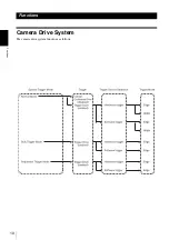
Page 10: ...Functions 10 Functions Camera Drive System The camera drive system functions as follows ...

Page 11: ...e trigger polarity before using other trigger functions Special Trigger Modes The three special trigger modes are Normal Bulk and Sequential triggering Normal trigger mode The Normal mode outputs images continuously according to internal continuous drive When trigger drive is enabled the camera is driven by either hardware or software triggering In this mode the following two drive methods are ava...

Page 12: ...ain values in different memory channels may result in different left and right video levels In such cases verify operation before use When using Bulk or Sequential trigger mode bear in mind that the following settings are ignored and have no effect Image Parameters Image Size H Image Size V Pixel Format Binning Test Chart Auto Gain Detection Frame ON OFF Auto Gain Detection Frame Area Setting Manu...

Page 13: ... 0 to 4 000 µs in 1 µs units GPO Outputs can be High or Low active Note When using strobe control output if the strobe delay or strobe width exceeds the exposure interval proper strobe signals cannot be output Set the strobe control output so that the delay and width are within the exposure time Gain The camera provides both manual and automatic gain control Manual gain control Variable gain contr...

Page 14: ...to 502 steps or 0 to 18 dB When setting Clamp L R and GainL R separately set the left side first Digital Gain The camera provides a digital gain function Gain values are from 1X to 2X 0 to 64 in 0 015625X increments Note When using digital gain discontinuity may occur in the spacing between output levels This occurs due to the lack of an image signal output that is equivalent to the output steps T...

Page 15: ... out position settings are specified with the following units Horizontal 8 pixel units Vertical 4 scan line units Note Be aware that the frame rate increases for vertical cut outs while the frame rate remains unchanged for horizontal cut outs Binning Mode This mode increases sensitivity and frame rate by combining vertically adjacent pixel data from the CCD Note Binning mode approximately doubles ...

Page 16: ...rdware triggering set only the trigger period to the displayed frame rate Image Acquisition Modes The following three image acquisition modes are available Continuous image output Output a user specified number of frames from 1 to 255 Single frame output Memory Channels and User Memories Memory channels Sixteen memory channels are provided for camera parameters that can be switched at each frame w...

Page 17: ...rivilege This mode specifies the control method 0 Ungoverned control No control commands are accepted from any application 1 Exclusive access One application has total control and other applications cannot even read registers 2 Control access One application has control and other applications can only read registers Notes If the Payload Size is set to a value smaller than the Packet Size images wi...

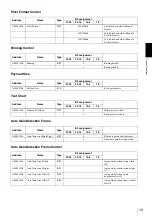
Page 18: ...ork Control Registers 0xA0000200 0xA0000214 Acquisition Control Registers 0xA0000220 0xA0000400 Feature Control Registers 0xA0001000 0xA0001008 Memory Control Registers 0xA0002000 0xA0002098 Feature Control Registers 0xA00020C0 0xA00020FC User Memory 0xA0007000 0xA0007090 Feature Control Inq 0xA0010000 0xA0013FFC LUT Look Up Table Control Register Address Name Type Bit assignment 31 24 23 16 15 8 ...

Page 19: ...ent 31 24 23 16 15 8 7 0 A0000120h Payload Size R O Read payload size Address Name Type Bit assignment 31 24 23 16 15 8 7 0 A0000130h Display Test Chart R W 0 Hide grayscale chart 1 Show grayscale chart Address Name Type Bit assignment 31 24 23 16 15 8 7 0 A0000134h Auto Gain Area High Light R W 0 Hide auto gain detection frame 1 Show auto gain detection frame Address Name Type Bit assignment 31 2...

Page 20: ... not use fixed IP address 1 Use fixed IP address Address Name Type Bit assignment 31 24 23 16 15 8 7 0 A0000190h Heartbeat Mode R W 0 Heartbeat disable 1 Heartbeat enable stops video image 2 Heartbeat enable stops video image and initialize network Address Name Type Bit assignment 31 24 23 16 15 8 7 0 A0000200h Acquisition Mode R W 1 Continuous frame transfer mode 2 Multi frame transfer mode 3 Sin...

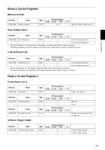
Page 21: ...nnel R W 0 15 Memory channel number select Address Name Type Bit assignment 31 24 23 16 15 8 7 0 A0001004h Save Parameters R W 1 Save camera parameters 2 Save common parameters Address Name Type Bit assignment 31 24 23 16 15 8 7 0 A0001008h Load Parameters R W 1 Load camera parameters 2 Load common parameters Address Name Type Bit assignment 31 24 23 16 15 8 7 0 A0000220h Frame Rate R W Frame rate...

Page 22: ...egative during special trigger mode Address Name Type Bit assignment 31 24 23 16 15 8 7 0 A0000300h Special Trigger Mode R W 0 Normal Mode setting 1 Bulk Mode setting 2 Sequential Mode setting Address Name Type Bit assignment 31 24 23 16 15 8 7 0 A0000304h Number Of Frames For Special Trigger Mode R W 1 16 Number of frames for special trigger mode Address Name Type Bit assignment 31 24 23 16 15 8 ...

Page 23: ...h Auto Clamp ON R W 0 Auto clamp disable 1 Execute one shot clamp setting 2 Auto clamp enable Address Name Type Bit assignment 31 24 23 16 15 8 7 0 A000201Ch Auto Gain ON R W 0 Auto gain disable 1 Execute one shot gain setting 2 Auto gain enable Address Name Type Bit assignment 31 24 23 16 15 8 7 0 A0002020h Auto Gain Level R W 0 Auto gain level setting Address Name Type Bit assignment 31 24 23 16...

Page 24: ...15 8 7 0 A0002048h Trigger Mode R W 0 Edge mode external trigger select 1 Width mode external trigger select Address Name Type Bit assignment 31 24 23 16 15 8 7 0 A000204Ch Trigger Polarity R W 0 Negative external trigger polarity 1 Positive external trigger polarity Address Name Type Bit assignment 31 24 23 16 15 8 7 0 A0002050h Trigger Inhibit R W 0 Permit external triggering 1 Inhibit external ...

Page 25: ...ess Name Type Bit assignment 31 24 23 16 15 8 7 0 A0002070h Strobe 1 Polarity R W 0 Negative Strobe 1 polarity 1 Positive Strobe 1 polarity Address Name Type Bit assignment 31 24 23 16 15 8 7 0 A0002074h Strobe 1 Delay R W Strobe 1 delay setting Address Name Type Bit assignment 31 24 23 16 15 8 7 0 A0002078h Strobe 1 Pulse Width R W Strobe 1 pulse width setting Address Name Type Bit assignment 31 ...

Page 26: ... 2 pulse width setting Address Name Type Bit assignment 31 24 23 16 15 8 7 0 A0002090h GPO R W Bit0 GPO 1 signal select Bit1 GPO 2 signal select Address Name Type Bit assignment 31 24 23 16 15 8 7 0 A0002098h Trigger Source Select R W 0 Hardware trigger source select 1 Software trigger source select Address Name Type Bit assignment 31 24 23 16 15 8 7 0 A00020C0h A00020FCh User Memory R W Memory av...

Page 27: ...04h Clamp R A0008F04h Clamp R A0008008h Gain L A0008F08h Gain L A000800Ch Gain R A0008F0Ch Gain R A0008010h Gain_dB L A0008F10h Gain_dB L A0008014h Gain_dB R A0008F14h Gain_dB R A0008018h Auto Clamp ON A0008F18h Auto Clamp ON A000801Ch Auto Gain ON A0008F1Ch Auto Gain ON A0008020h Auto Gain Level A0008F20h Auto Gain Level A0008034h Digital A0008F34h Digital A0008038h Pedestal A0008F38h Pedestal A0...

Page 28: ...h Strobe 2 Delay A0008F88h Strobe 2 Delay A000808Ch Strobe 2 Pulse Width A0008F8Ch Strobe 2 Pulse Width A0008090h GPO Output A0008F90h GPO Output A0008094h Software Trigger Signal A0008F94h Software Trigger Signal A0008098h Trigger Source Select A0008F98h Trigger Source Select A00080C0h A00080FCh User Memory A0008FC0h A0008FFCh User Memory Memory channel 0 Memory channel 15 Address Name Address Na...

Page 29: ... 0xA0000120 Payload Size R O 0xA0000130 Test Chart R W 0 0xA0000134 Auto Gain Area R W 0 0xA0000138 Auto Gain Area Width R W 50 0xA000013C Auto Gain Area Height R W 50 0xA0000140 Auto Gain Area Offset X R W 25 0xA0000144 Auto Gain Area Offset Y R W 25 Address Name Type Value V60E SX97E U100E 5005E 0xA0000180 Bandwidth MBps R W 50 0xA0000184 Packet Size R W 6000 0xA0000188 DHCP R W 1 0xA000018C Per...

Page 30: ...hannel R W 0 0xA0001004 Save Parameters R W 0 0xA0001008 Load Parameters R W 0 Address Name Type Value V60E SX97E U100E 5005E 0xA0002000 Clamp L R W 0xA0002004 Clamp R R W 0xA0002008 Gain L R W 0 0xA000200C Gain R R W 0 0xA0002010 Gain_dB L R W 0 0xA0002014 Gain_dB R R W 0 0xA0002018 Auto Clamp ON R W 1 0xA000201C Auto Gain ON R W 0 0xA0002020 Auto Gain Level R W 11264 0xA0002034 Digital R W 1 0xA...

Page 31: ...dth R W 0 0xA0002080 Strobe 2 Mode R W 0 0xA0002084 Strobe 2 Polarity R W 0 0xA0002088 Strobe 2 Delay R W 0 0xA000208C Strobe 2 Pulse Width R W 0 0xA0002090 GPO Output R W 0 0xA0002098 Trigger Source Select R W 0 0xA00020C0 User Memory R W 0 0xA00020FC R W 0 Address Name Type Value V60E SX97E U100E 5005E ...

Page 32: ...Min R O 0 A0007038h Auto Gain Area Max R O 100 A000703Ch Auto Gain Area Min R O 0 A0007040h Auto Gain Offset Max R O 100 A0007044h Auto Gain Offset Min R O 0 A0007048h Pedestal Max R O 2047 A000704Ch Pedestal Min R O 0 A0007050h Digital Gain Max R O 128 A0007054h Digital Gain Min R O 0 A0007058h Shutter Max R O 2000000 A000705Ch Shutter Min R O 10 A0007060h Trigger Delay Max R O 4000 A0007064h Tri...

Page 33: ...hutter speed 2 to 1 100 000 s External trigger shutter Edge width mode software trigger via 1000BASE T bulk trigger sequential trigger trigger inhibit trigger strobe delay Lens mount C mount Flange back 17 526 mm Minimum illumination 1 lx Iris F1 4 Gain 18 dB Shutter 11 046 µs 0 2 lx Iris F1 4 Gain 18 dB Shutter 60 000 µs 1 lx Iris F1 4 Gain 18 dB Shutter 66 506 µs 1 lx Iris F1 4 Gain 18 dB Shutte...

Page 34: ...m 0 0 0 1 0 2 0 3 0 4 0 5 0 6 0 7 0 8 0 9 1 0 400 500 600 700 800 900 1000 Camera Relative Response Without lens and light source parameters Wave Length nm 0 0 0 1 0 2 0 3 0 4 0 5 0 6 0 7 0 8 0 9 1 0 400 500 600 700 800 900 1000 Camera Relative Response Without lens and light source parameters Wave Length nm 0 0 0 1 0 2 0 3 0 4 0 5 0 6 0 7 0 8 0 9 1 0 400 500 600 700 800 900 1000 Camera Relative R...

Page 35: ...Appendix 35 Dimensions Unit mm inches 2 M3 depth 4 2 M3 depth 3 16 4 M3 depth 4 4 M3 depth 3 16 2 M2 depth 2 6 2 M2 depth 1 8 2 M2 depth 4 2 M2 depth 3 16 ...

Page 36: ... information contained herein is for reference only and does not convey any license by any implication or otherwise under any intellectual property right or other right of Sony or third parties Sony cannot assume responsibility for any right infringements arising out of the use of this information Sony Corporation ...

Reviews: