98
STR-DA3000ES
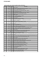
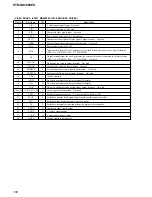
Pin No.
Pin Name
I/O
Description
55
VSS
—
Ground terminal
56 to 58
D21 to D19
I/O
Two-way data bus with the S-RAM
59
A11
O
Address signal output to the S-RAM
60, 61
SDO1, SDO2
O
Audio serial data output to the lip sync adjust
62
KFSIO
I
Audio clock signal input from the digital audio interface receiver
63
LRCKO
O
L/R sampling clock signal (44.1 kHz) output terminal
64
BCKO
O
Bit clock signal (2.8224 MHz) output terminal
65
VDDI
—
Power supply terminal (+2.5V)
66
VSS
—
Ground terminal
67, 68
D18, D17
I/O
Two-way data bus with the S-RAM
69, 70
A10, A9
O
Address signal output to the S-RAM
71
CAS
O
Column address strobe signal output terminal Not used
72
RAS
O
Row address strobe signal output terminal Not used
73
VDDI
—
Power supply terminal (+2.5V)
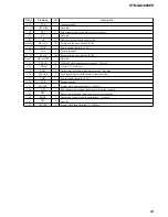
74
HDIN
I
Serial data input from the main system controller
75
HCLK
I
Serial data transfer clock signal input from the main system controller
76
HCS
I
Chip select signal input from the main system controller
77, 78
A8, A7
O
Address signal output to the S-RAM
79, 80
D16, D15
I/O
Two-way data bus with the S-RAM
81
VSS
—
Ground terminal
82
HDOUT
O
Serial data output to the main system controller
83
HACN
O
Acknowledge signal output to the main system controller
84
CSO
O
Chip select signal output to the S-RAM
85
WEO
O
Write enable signal output to the S-RAM
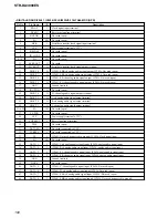
86
A6
O
Address signal output to the S-RAM
87 to 89
D14 to D12
I/O
Two-way data bus with the S-RAM
90
VDDE
—
Power supply terminal (+3.3V)
91
VSS
—
Ground terminal
92 to 94
D11 to D9
I/O
Two-way data bus with the S-RAM
95
A5
O
Address signal output to the S-RAM
96
VDDI
—
Power supply terminal (+2.5V)
97
TCK
I
Simplicity emulation clock signal input terminal Not used
98
TDI
I
Simplicity emulation data input terminal Not used
99
TDO
O
Simplicity emulation data input terminal Not used
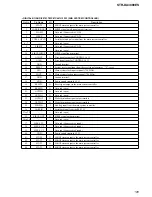
100
TMS
I
Simplicity emulation data input start and end select Not used
101
XTRST
I
Simplicity emulation non-sync break signal input terminal Not used
102
VSS
—
Ground terminal
103, 104
D8, D7
I/O
Two-way data bus with the S-RAM
105, 106
A4, A3
O
Address signal output to the S-RAM
107, 108
GP10, GP9
—
Not used
109
VDDI
—
Power supply terminal (+2.5V)
110
GP8
—
Not used
111
GP7
I
L/R sampling clock signal (44.1 kHz) input terminal
112
GP6
—
Not used
113, 114
A2, A1
O
Address signal output to the S-RAM
115, 116
D6, D5
I/O
Two-way data bus with the S-RAM


