background image

– 18 –

5-1.

BASE  UNIT

[Start-up]

1. Set the 

[DIAL MODE]

 switch to the P (PULSE) side.

2. Keeping the 

[INTERCOM]

 button pressed, turn the power on.

3. After a start-up acknowledge tone sounds, set the 

[DIAL MODE]

switch from P (PULSE) to T (TONE) side, then return to the P
(PULSE) side.

4. Release the

[INTERCOM]

 button, and the Test Mode will start.

5. Allow for normal ringer to sound at high level for duration of

500 msec after start-up, then close the line and dial Pause 

 0

(DP) 

   (mode change) 

 1 (tone) 

 4 (tone) 

 8 (tone)

 # (tone).

6. After dialing, the base unit will go in Test Mode Idle status.

[Ring Detection Test]

1. The LINE LED blinks in synchronization with the RING sig-

nal and at the same time, Normal Ringer sounds, if the RING
signal is detected in the Test Mode Idle status.

[Charge Detection • ARTO Output Test]

1. Square-wave signal (2.4 kHz) is output to the IC751 pin 

(ARTO terminal) when the CHARGE signal is detected (IC751
pin 

^™

 (PARKP terminal) H 

 L) in the Test Mode Idle sta-

tus.

2. At this time, the EEPROM (IC951) is reset.

[Charge Control Test]

1. IC751 pin 

 (CHG-HIGH RATE terminal) outputs H 

 L 

H once, if IC751 pin 

 (VCHG-MON terminal) changes to H

 L 

 H when the CHARGE signal is detected in the Test

Mode Idle status.

[Test Mode by Manual Input]

• The key input in the Test Mode Idle status can change the set

status to the following modes. However, the transition to an-
other mode within respective test mode groups (A-J) is possible
directly, but in case of transition to other test mode group, the
set must be returned to the Test Mode Idle status once by enter-
ing the command “0-1-#”.

A) Test mode termination

Command

Mode/Operation

0-0-#

Terminate the Test mode.

B) Return test mode idle

Command

Mode/Operation

0-1-#

Return to Test Mode Idle status.

C) Continuous receiving test group (Note 1)

Command

Mode/Operation

1-1-#

CH1 continuous receiving status (LNA, AGC ON)

D) Continuous transmission test group (Note 1)

Command

Mode/Operation

2-1-#

CH1 continuous transmission status (TX Power High)

2-2-#

CH1 continuous transmission status (TX Power Mid)

2-3-#

CH1 continuous transmission status (TX Power Low)

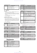
Note 1:

Each time the 

[*]

 key is pressed, the channels change over as

follows:

CH1 

 CH2 

 CH3 


 CH20

SECTION  5

TEST MODE

E) Loopback test group 1

Command

Mode/Operation

3-1-#

CODEC Forward Loopback (L1)
(Speech path: Talk status)
(LINE IN 

 LINE OUT: CODEC LINE IN

 SPKR OUT)

3-2-#

ADPCM Forward Loopback (L2)
(Speech path: Talk status)
(LINE IN 

 CODEC 

 ADPCM 

 CODEC 

 LINE OUT)

3-3-#

ADPCM 

 RF Loopback

(Speech path: Talk status)
(LINE IN 

 CODEC 

 ADPCM 

 RF 

 ADPCM


  CODEC 

 LINE OUT)

F) TDD test group 1

Command

Mode/Operation

4-1-#

CH1 TDD mode (Master timing, Power High) status

4-2-#

CH1 TDD mode (Master timing, Power Mid) status

4-3-#

CH1 TDD mode (Master timing, Power Low) status

4-4-#

TDD mode (Slave timing, Standby) status. Power

(Note 2)

control

Note 2:

To make a speech with the handset, first operate the  set in Slave
mode by “4-4-#” command, and operate the counterpart in the
Master mode by “6-1-#” command. However, the ID must be
same. To set the same ID, perform ON-Charge in advance, or
clear the EEPROM by “7-1-#” command. In this case, however,
the speech path should be the intercom status.

G) MMI test group

Command

Mode/Operation

5-1-#

Key test.

•  Press the keys successively in the following

order:

[PGM]


[SPEED DIAL]


[REDIAL/PAUSE]


[FLASH]


[1]


[2]


[3]


[4]


[5]


[6]


[7]


[8]


[9]


[*]


[0]


[#]


[INTERCOM]


[HOLD]


[SPEAKERPHONE]

• If key input sequence is correct: An acknowl-

edge tone sounds, and the set returns to the Test
Mode Idle status.

• If key input sequence is wrong: An error tone

sounds, and the set returns to the Test Mode
Idle status.

5-3-#

LCD test.
All dots on LCD lights up immediately when the LCD
test mode is selected.

5-4-#

LED test.

[NEW CALL]

 and 

[LINE]

 LEDs lights up

immediately when the LED test mode is selected.

H) TDD test group 2

Command

Mode/Operation

6-1-#

TDD mode (Master timing) status. Power control.

Refer to the description of “4-4-#” command.

I) Memory clear test group

Command

Mode/Operation

7-1-#

The contents of EEPROM are cleared. In case of
successful clear, an acknowledge tone sounds.

www. xiaoyu163. com

QQ 376315150

9

9

2

8

9

4

2

9

8

TEL 13942296513

9

9

2

8

9

4

2

9

8

0

5

1

5

1

3

6

7

3

Q

Q

TEL  13942296513  QQ  376315150  892498299 

TEL  13942296513  QQ  376315150  892498299 

http://www.xiaoyu163.com

http://www.xiaoyu163.com

Summary of Contents for SPP-SS965 - Cordless Telephone

Page 1: ...x 58 x 177 x 46 mm w h d antenna excluded approx 2 3 8 x 7 x 1 13 16 inches Antenna Approx 72 mm approx 2 7 8 inches Mass Approx 250 g approx 8 8 oz battery included Base phone Power source DC 9V from AC power adaptor AC T46 Battery charging time Approx 12 hours Dimensions Approx 170 x 60 x 214 mm w h d antenna excluded approx 6 3 4 x 2 3 8 x 8 1 2 inches Antenna Approx 165 mm approx 6 1 2 inches ...

Page 2: ... 7 10 Printed Wiring Board BASE KEY Section 45 7 11 Schematic Diagram BASE KEY Section 46 7 12 Printed Wiring Board BASE LCD Section 47 7 13 Schematic Diagram BASE LCD Section 48 7 14 Printed Wiring Board HAND MAIN Section 49 7 15 Schematic Diagram HAND MAIN Section 51 7 16 IC Pin Function Description 55 8 EXPLODED VIEWS 61 9 ELECTRICAL PARTS LIST 63 Notes on chip component replacement Never reuse...

Page 3: ...cables with tapes at G to L positions Cable fasting direction Cable fasting direction OK NG Note Make sure the wires do not rise above the sponge and shield plate A G L K F J E D I C D E H B Note Tape over the diode D1001 Note Make sure the wires do not rise black red 90 white Cable fasting direction clamp stopper 2 c m www xiaoyu163 com QQ376315150 9 9 2 8 9 4 2 9 8 TEL 13942296513 9 9 2 8 9 4 2 ...

Page 4: ...rom instruction manual www xiaoyu163 com QQ376315150 9 9 2 8 9 4 2 9 8 TEL 13942296513 9 9 2 8 9 4 2 9 8 0 5 1 5 1 3 6 7 3 Q Q TEL 13942296513 QQ 376315150 892498299 TEL 13942296513 QQ 376315150 892498299 http www xiaoyu163 com http www xiaoyu163 com ...
Page 5: ...63 com QQ376315150 9 9 2 8 9 4 2 9 8 TEL 13942296513 9 9 2 8 9 4 2 9 8 0 5 1 5 1 3 6 7 3 Q Q TEL 13942296513 QQ 376315150 892498299 TEL 13942296513 QQ 376315150 892498299 http www xiaoyu163 com http www xiaoyu163 com ...
Page 6: ...63 com QQ376315150 9 9 2 8 9 4 2 9 8 TEL 13942296513 9 9 2 8 9 4 2 9 8 0 5 1 5 1 3 6 7 3 Q Q TEL 13942296513 QQ 376315150 892498299 TEL 13942296513 QQ 376315150 892498299 http www xiaoyu163 com http www xiaoyu163 com ...
Page 7: ...63 com QQ376315150 9 9 2 8 9 4 2 9 8 TEL 13942296513 9 9 2 8 9 4 2 9 8 0 5 1 5 1 3 6 7 3 Q Q TEL 13942296513 QQ 376315150 892498299 TEL 13942296513 QQ 376315150 892498299 http www xiaoyu163 com http www xiaoyu163 com ...
Page 8: ...63 com QQ376315150 9 9 2 8 9 4 2 9 8 TEL 13942296513 9 9 2 8 9 4 2 9 8 0 5 1 5 1 3 6 7 3 Q Q TEL 13942296513 QQ 376315150 892498299 TEL 13942296513 QQ 376315150 892498299 http www xiaoyu163 com http www xiaoyu163 com ...
Page 9: ...63 com QQ376315150 9 9 2 8 9 4 2 9 8 TEL 13942296513 9 9 2 8 9 4 2 9 8 0 5 1 5 1 3 6 7 3 Q Q TEL 13942296513 QQ 376315150 892498299 TEL 13942296513 QQ 376315150 892498299 http www xiaoyu163 com http www xiaoyu163 com ...
Page 10: ...63 com QQ376315150 9 9 2 8 9 4 2 9 8 TEL 13942296513 9 9 2 8 9 4 2 9 8 0 5 1 5 1 3 6 7 3 Q Q TEL 13942296513 QQ 376315150 892498299 TEL 13942296513 QQ 376315150 892498299 http www xiaoyu163 com http www xiaoyu163 com ...
Page 11: ...63 com QQ376315150 9 9 2 8 9 4 2 9 8 TEL 13942296513 9 9 2 8 9 4 2 9 8 0 5 1 5 1 3 6 7 3 Q Q TEL 13942296513 QQ 376315150 892498299 TEL 13942296513 QQ 376315150 892498299 http www xiaoyu163 com http www xiaoyu163 com ...
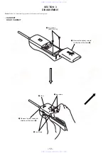
Page 12: ...ery case lid to direction of the arrow A A 4 claw 3 two claws 3 two claws 5 Remove the rear cabinet to direction of the arrow B B www xiaoyu163 com QQ376315150 9 9 2 8 9 4 2 9 8 TEL 13942296513 9 9 2 8 9 4 2 9 8 0 5 1 5 1 3 6 7 3 Q Q TEL 13942296513 QQ 376315150 892498299 TEL 13942296513 QQ 376315150 892498299 http www xiaoyu163 com http www xiaoyu163 com ...
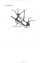
Page 13: ...screws BTP2 6 8 4 Removal of the HAND MAIN board direction of the arrow A A www xiaoyu163 com QQ376315150 9 9 2 8 9 4 2 9 8 TEL 13942296513 9 9 2 8 9 4 2 9 8 0 5 1 5 1 3 6 7 3 Q Q TEL 13942296513 QQ 376315150 892498299 TEL 13942296513 QQ 376315150 892498299 http www xiaoyu163 com http www xiaoyu163 com ...
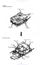
Page 14: ... four screws P3 16 1 four screws BTP2 6 8 4 connector CN202 4 connector CN601 3 connector CN802 3 connector CN801 www xiaoyu163 com QQ376315150 9 9 2 8 9 4 2 9 8 TEL 13942296513 9 9 2 8 9 4 2 9 8 0 5 1 5 1 3 6 7 3 Q Q TEL 13942296513 QQ 376315150 892498299 TEL 13942296513 QQ 376315150 892498299 http www xiaoyu163 com http www xiaoyu163 com ...
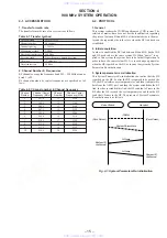
Page 15: ...n the RF link has been established 2 Initial acquisition In order to establish the RF link between BS and HS both of BS and HS need to have the same system ID When power is ap plied to this system the system have to do Initial Acquisition in order to have the same system ID It is to exchange a parameter when the HS is parked on the BS as soon as the system do System Parameters Re initialization 3 ...

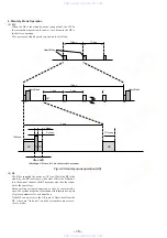
Page 16: ...rfer ence the system needs the clear channel information as a part of system parameter for a channel hop If the BS can not receive the A Frame of Heart beat from the HS it become link error and the system become error re covery mode 10 sec 10 sec Heart Beat Heart Beat 1 sec 1 sec RX RX RX RX RX RX 1 sec 2 msec 2 msec 10 msec 10 msec RX TX RX Heart Beat Exchange A Frame for Link confirmation purpos...

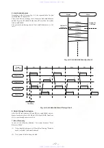
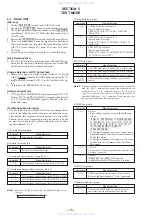
Page 17: ...ecovery In case of the following situation The system becomes Error Recovery Mode 1 The system failed to move to Heart Beat during Stand by mode or failed link establishment 2 The system failed to keep the link Fig 4 3 Link Establishment protocol Master Slave System ID confirmed System ID confirmed A Frame A Frame V Frame V Frame V Frame V Frame Fig 4 4 Link Establishment Timing Chart Master TX Ma...

Page 18: ...Power Mid 2 3 CH1 continuous transmission status TX Power Low Note 1 Each time the key is pressed the channels change over as follows CH1 CH2 CH3 CH20 SECTION 5 TEST MODE E Loopback test group 1 Command Mode Operation 3 1 CODEC Forward Loopback L1 Speech path Talk status LINE IN LINE OUT CODEC LINE IN SPKR OUT 3 2 ADPCM Forward Loopback L2 Speech path Talk status LINE IN CODEC ADPCM CODEC LINE OUT...

Page 19: ... 5 2 HANDSET Start up 1 With the power supplied press TALK 0 and 1 keys simul taneously and the Test Mode will start 2 Allow for normal ringer to sound at high level for duration of 500 msec after start up then the handset will go in Test Mode Idle status 3 The RF in Talk Intercom status is as follows TALK LED lights up Test Mode by Manual Input The key input in the Test Mode Idle status can chang...

Page 20: ...ance becomes shorter will increase Measuring process Setting Spectrum analyzer Center frequency 903 6 MHz CH1 RBW 30 kHz VBW 30 kHz Span 3 MHz or 5MHz Setting Test mode Continuous Transmit mode CH1 High Power Refer to Test Mode on page 18 Measurement Measure transmitting wave Specifications Acceptable level XdB difference between the highest peak and the lowest peak of odd side band the first to s...

Page 21: ... 81 2 3 70 20 36 33 75 1 52 18 33 30 79 3 4 47 21 48 34 78 4 36 18 65 33 3 4 4 64 21 85 35 12 4 25 19 37 33 05 5 4 52 21 18 35 54 2 35 19 05 32 95 6 4 02 21 57 35 12 2 96 19 14 33 45 7 5 03 22 14 35 45 4 12 19 12 33 01 8 5 58 22 35 35 61 2 89 18 56 32 12 9 4 03 21 32 35 82 5 01 18 33 32 41 10 4 43 19 69 33 92 2 74 17 28 31 33 4 435 21 29 34 96 3 256 18 7 32 52 σ 0 5336 0 7634 0 6747 1 0562 0 5895 ...

Page 22: ...ND on the BASE MAIN board in the base unit 2 Place the base unit in the Continuous Transmit mode CH1 High power 3 Measure the ANT OUT frequency of the RF module in the base unit using a frequency counter 4 Confirm that the measured frequency is 903 600 MHz 27 kHz 3 Checking TX Output Setting Procedure 1 Place the base unit in the Continuous Transmit mode CH1 High power 2 Measure the ANT OUT output...

Page 23: ...ace the handset in the Continuous Transmit mode CH1 High power 3 Measure theANT OUT frequency of the RF module in the hand set using a frequency counter 4 Confirm that the measured frequency is 903 600 MHz 27 kHz 5 Also execute steps 1 through 4 for the channels 10 and 20 level meter oscilloscope TP520 RXIP TP521 RXIN TP522 RXQP TP523 RXQN TP553 GND SSG ANTENNA TERMINAL frequency counter ANTENNA T...

Page 24: ... 8 1 CN901 16 1 CN902 ANT RF UNIT SW951 P T ANTENNA TERMINAL SSG Checking RX I Q Output level frequency counter Checking TX Center Frequency peak power meter Checking TX Output www xiaoyu163 com QQ376315150 9 9 2 8 9 4 2 9 8 TEL 13942296513 9 9 2 8 9 4 2 9 8 0 5 1 5 1 3 6 7 3 Q Q TEL 13942296513 QQ 376315150 892498299 TEL 13942296513 QQ 376315150 892498299 http www xiaoyu163 com http www xiaoyu163...
Page 25: ...TENNA TERMINAL SSG Checking RX I Q Output level frequency counter Checking TX Center Frequency peak power meter Checking TX Output CN501 S502 w w w x i a o y u 1 6 3 c o m Q Q 3 7 6 3 1 5 1 5 0 9 9 2 8 9 4 2 9 8 T E L 1 3 9 4 2 2 9 6 5 1 3 9 9 2 8 9 4 2 9 8 0 5 1 5 1 3 6 7 3 Q Q TEL 13942296513 QQ 376315150 892498299 TEL 13942296513 QQ 376315150 892498299 http www xiaoyu163 com http www xiaoyu163 ...
Page 26: ...TX DATA TXPWR0 TXPWR1 TXEN TXDATA TXPWR0 Q751 Q750 751 TX POWER ATTENUATOR Q750 TXPWR1 TXEN B P F B P F BRANCH DET RXO VO1 RXI 94 22 VIN 4 5 VO2 CD 8 1 VLC 13 21 HOOK ON OFF CONTROL Q207 VBAT FOR PLL VBAT FOR TX CN902 TXRXSW SYNDATA SYNCLK 10 2 7 4 5 6 12 11 SYNSTB 13 SYNEN 15 REFOSC TXRXSEL SYNDATA SYNCLK SYNSTB SYNEN SYNTH5MCLK 14 3 49 85 80 79 82 65 71 DATA DCLK FSKEN 17 16 15 20 70 61 93 69 72...

Page 27: ...1 22 10 15 6 9 CHG HIGH RATE 5V REGULATOR IC603 5V REGULATOR IC601 CHARGE CONTROL Q651 652 654 CHARGE DETECT Q653 LEVEL SHIFT Q852 QUICK NORMAL CHARGE CONTROL Q601 655 62 87 ARTO 34 D1001 CHARGE AUDIO SYSTEM B DIGITAL SYSTEM B CHARGE TERMINAL J601 DC IN 9V PARKP ART ASIC IC751 2 2 B LCD R W LCD REG SET LCDCS LIQUID CRYSTAL DISPLAY UNIT LCD801 78 67 w w w x i a o y u 1 6 3 c o m Q Q 3 7 6 3 1 5 1 5...

Page 28: ...T FOR TX CN502 TXRXSW SYNDATA SYNCLK 10 2 7 4 5 6 12 11 SYNSTB 13 SYNEN 15 REFOSC TXRXSEL SYNDATA SYNCLK SYNSTB SYNEN SYNTH5MCLK 14 3 49 85 80 79 82 65 71 72 75 66 NVDI NVDO SKDI DO 76 77 X501 9 6MHz XTALO XTALI 97 98 5 6 SPEAKER AMP LINE AMP LINEO 17 SPKPO 19 LEVEL SHIFT Q503 SPKMO 18 KEYPADI0 KEYPADI5 10 15 KEYPADB0 KEYPADB3 36 35 31 22 RINGOFF BATT SAVE RING ON S501 BATT SAVE RING ON KEY MATRIX...

Page 29: ...with regulated dc power supply from battery terminal CN301 on the HAND MAIN board Voltages and waveforms are dc with respect to ground in test mode Voltages are taken with aVOM Input impedance 10 MΩ Voltage variations may be noted due to normal produc tion tolerances Waveforms are taken with a oscilloscope Voltage variations may be noted due to normal produc tion tolerances Circled numbers refer t...

Page 30: ...ide A BASE MICROPHONE Board Semiconductor Location SIDE A Ref No Location Page 37 Page 47 Page 45 w w w x i a o y u 1 6 3 c o m Q Q 3 7 6 3 1 5 1 5 0 9 9 2 8 9 4 2 9 8 T E L 1 3 9 4 2 2 9 6 5 1 3 9 9 2 8 9 4 2 9 8 0 5 1 5 1 3 6 7 3 Q Q TEL 13942296513 QQ 376315150 892498299 TEL 13942296513 QQ 376315150 892498299 http www xiaoyu163 com http www xiaoyu163 com ...
Page 31: ...02 E 9 Q203 F 10 Q204 F 10 Q206 D 11 Q207 D 10 Q212 G 11 Q213 H 11 Q214 G 9 Q215 G 9 Q216 I 10 Q217 D 10 Q601 I 8 Q651 H 8 Q652 I 8 Q653 I 7 Q654 I 9 Q655 I 9 Q750 C 5 Q751 B 4 Q852 H 10 37 38 Semiconductor Location SIDE B Ref No Location 7 6 PRINTED WIRING BOARD BASE MAIN Board Side B Page 35 w w w x i a o y u 1 6 3 c o m Q Q 3 7 6 3 1 5 1 5 0 9 9 2 8 9 4 2 9 8 T E L 1 3 9 4 2 2 9 6 5 1 3 9 9 2 8...

Page 32: ... Diagrams Page 46 Page 43 Page 43 Page 41 Page 48 w w w x i a o y u 1 6 3 c o m Q Q 3 7 6 3 1 5 1 5 0 9 9 2 8 9 4 2 9 8 T E L 1 3 9 4 2 2 9 6 5 1 3 9 9 2 8 9 4 2 9 8 0 5 1 5 1 3 6 7 3 Q Q TEL 13942296513 QQ 376315150 892498299 TEL 13942296513 QQ 376315150 892498299 http www xiaoyu163 com http www xiaoyu163 com ...
Page 33: ...for IC Block Diagrams Page 40 Page 43 w w w x i a o y u 1 6 3 c o m Q Q 3 7 6 3 1 5 1 5 0 9 9 2 8 9 4 2 9 8 T E L 1 3 9 4 2 2 9 6 5 1 3 9 9 2 8 9 4 2 9 8 0 5 1 5 1 3 6 7 3 Q Q TEL 13942296513 QQ 376315150 892498299 TEL 13942296513 QQ 376315150 892498299 http www xiaoyu163 com http www xiaoyu163 com ...
Page 34: ...rams Page 40 Page 39 Page 41 w w w x i a o y u 1 6 3 c o m Q Q 3 7 6 3 1 5 1 5 0 9 9 2 8 9 4 2 9 8 T E L 1 3 9 4 2 2 9 6 5 1 3 9 9 2 8 9 4 2 9 8 0 5 1 5 1 3 6 7 3 Q Q TEL 13942296513 QQ 376315150 892498299 TEL 13942296513 QQ 376315150 892498299 http www xiaoyu163 com http www xiaoyu163 com ...
Page 35: ...en Carbon pattern Pattern from the side which enables seeing Page 35 www xiaoyu163 com QQ376315150 9 9 2 8 9 4 2 9 8 TEL 13942296513 9 9 2 8 9 4 2 9 8 0 5 1 5 1 3 6 7 3 Q Q TEL 13942296513 QQ 376315150 892498299 TEL 13942296513 QQ 376315150 892498299 http www xiaoyu163 com http www xiaoyu163 com ...

Page 36: ...Y Section Page 39 www xiaoyu163 com QQ376315150 9 9 2 8 9 4 2 9 8 TEL 13942296513 9 9 2 8 9 4 2 9 8 0 5 1 5 1 3 6 7 3 Q Q TEL 13942296513 QQ 376315150 892498299 TEL 13942296513 QQ 376315150 892498299 http www xiaoyu163 com http www xiaoyu163 com ...
Page 37: ...LCD Section Page 35 Page 40 w w w x i a o y u 1 6 3 c o m Q Q 3 7 6 3 1 5 1 5 0 9 9 2 8 9 4 2 9 8 T E L 1 3 9 4 2 2 9 6 5 1 3 9 9 2 8 9 4 2 9 8 0 5 1 5 1 3 6 7 3 Q Q TEL 13942296513 QQ 376315150 892498299 TEL 13942296513 QQ 376315150 892498299 http www xiaoyu163 com http www xiaoyu163 com ...

Page 38: ... MAIN Section Semiconductor Location SIDE A Ref No Location D502 B 3 D503 B 3 Q501 A 3 Q504 C 2 Q505 C 2 Semiconductor Location SIDE B Ref No Location Note carbon pattern w w w x i a o y u 1 6 3 c o m Q Q 3 7 6 3 1 5 1 5 0 9 9 2 8 9 4 2 9 8 T E L 1 3 9 4 2 2 9 6 5 1 3 9 9 2 8 9 4 2 9 8 0 5 1 5 1 3 6 7 3 Q Q TEL 13942296513 QQ 376315150 892498299 TEL 13942296513 QQ 376315150 892498299 http www xiao...

Page 39: ...ge 54 for IC Block Diagrams w w w x i a o y u 1 6 3 c o m Q Q 3 7 6 3 1 5 1 5 0 9 9 2 8 9 4 2 9 8 T E L 1 3 9 4 2 2 9 6 5 1 3 9 9 2 8 9 4 2 9 8 0 5 1 5 1 3 6 7 3 Q Q TEL 13942296513 QQ 376315150 892498299 TEL 13942296513 QQ 376315150 892498299 http www xiaoyu163 com http www xiaoyu163 com ...
Page 40: ... 4 VCC 3 CD FO 5 9 8 7 6 HTI TXO TXI HTO HTO 10 12 11 14 13 27 28 25 26 24 20 21 22 23 19 17 18 15 16 MUT MCO MCI CT VLC VR VCC HYBRID AMP 2 HYBRID AMP 1 MIC AMP VREF VR FILTER AMP COMPARATOR AGC BACKGROUND NOISE DETECTOR VR LEVEL DETECTOR LEVEL DETECTOR COMPARATOR ATTENUATOR CONTROL BLOCK BACKGROUND NOISE DETECTOR DIAL TONE DETECTOR LEVEL DETECTOR LEVEL DETECTOR RX ATTEN UATOR TX ATTENUATOR IC150...

Page 41: ...r supply terminal 5V for pad 30 VSSP Ground terminal for pad 31 KEYPADB2 O Key send signal output to the key matrix 32 CDCFRAME O Frame output to the CODEC IC401 33 ARTI I ART input from the base unit 34 ARTO O ART output terminal Not used open 35 36 KEYPADB1 KEYPADB0 O Key send signal output to the key matrix 37 GPIOB7 O Not used open 38 VDDP Power supply terminal 5V for pad 39 LCDCS O Chip selec...

Page 42: ...wer control signal output to the RF unit H enable 76 NVDI I O Two way data bus with the EEPROM IC502 77 NVDO O Clock signal output to the EEPROM IC502 78 LCDRW O Data read write selection signal output to the liquid crystal display unit LCD501 L data write H data read 79 TXEN O TX system enable signal output to the RF unit H enable 80 TXPWR1 O PA power selection signal output to the RF unit 81 GPI...

Page 43: ...hanges to H 97 XTALI I Main system clock input terminal 9 6 MHz 98 XTALO O Main system clock output terminal 9 6 MHz 99 VDDP Power supply terminal 5V for pad 100 VSSP Ground terminal for pad www xiaoyu163 com QQ376315150 9 9 2 8 9 4 2 9 8 TEL 13942296513 9 9 2 8 9 4 2 9 8 0 5 1 5 1 3 6 7 3 Q Q TEL 13942296513 QQ 376315150 892498299 TEL 13942296513 QQ 376315150 892498299 http www xiaoyu163 com http...
Page 44: ...RAME O Frame output to the CODEC IC701 33 ARTI I ART input terminal Not used fixed at H 34 ARTO O ART output to the handset unit 35 36 KEY OUT1 KEY OUT0 O Key send signal output to the key matrix 37 OFFHOOK O Hook on off control signal output terminal L on hook H off hook 38 VDDP Power supply terminal 5V for pad 39 LCDCS O Chip select signal output to the liquid crystal display unit LCD801 40 VDDC...

Page 45: ...d 79 TXEN O TX system enable signal output to the RF unit H enable 80 TXPWR1 O PA power selection signal output to the RF unit 81 RINGIN I Detection signal input of the ringer coming L ringer coming 82 TXRXSEL O TX RX selection signal output to the RF unit L RX H TX 83 VCHG MON I Battery charge monitor input terminal 84 BASEP I Setting terminal for the base handset selection L base unit H handset ...

Page 46: ...t terminal 9 6 MHz 99 VDDP Power supply terminal 5V for pad 100 VSSP Ground terminal for pad www xiaoyu163 com QQ376315150 9 9 2 8 9 4 2 9 8 TEL 13942296513 9 9 2 8 9 4 2 9 8 0 5 1 5 1 3 6 7 3 Q Q TEL 13942296513 QQ 376315150 892498299 TEL 13942296513 QQ 376315150 892498299 http www xiaoyu163 com http www xiaoyu163 com ...
Page 47: ...5 01 HOLDER SP 4 3 012 363 11 CABINET REAR 5 X 3375 670 1 LID ASSY BATTERY CASE 6 3 022 150 01 LABEL NI CD RECYCLE 7 A 3622 209 A HAND MAIN BOARD COMPLETE 8 1 771 066 21 SWITCH RUBBER KEY HAND 9 3 012 366 01 TERMINAL HAND CHARGE 10 3 935 519 21 CUSHION BUZZER 11 3 935 519 11 CUSHION BUZZER 12 3 935 520 01 CUSHION BATTERY 13 3 028 552 01 SHEET COPPER LEAF RF 14 3 029 168 01 SHEET COPPER LEAF RF B 1...

Page 48: ...066 02 SHEET COPPER LEAF RF C 66 3 936 696 21 FOOT RUBBER 67 X 3375 888 1 CABINET LOWER ASSY 68 3 026 909 01 SHEET RESET BUTTON 69 3 032 727 01 CUSHION for PWB B 70 1 671 564 11 BASE LCD BOARD 71 3 024 961 01 FRAME LCD 72 3 026 188 01 ILLUMINATOR SS965 73 3 024 960 01 HOLDER LCD ANT901 1 501 998 11 ANTENNA ROD LCD801 1 475 724 11 LCD UNIT RFU901 1 475 890 11 RF UNIT SP101 1 505 802 11 SPEAKER 5 7c...

Page 49: ...3 1 216 033 00 METAL CHIP 220 5 1 10W R814 1 216 033 00 METAL CHIP 220 5 1 10W R819 1 216 025 00 RES CHIP 100 5 1 10W R820 1 216 033 00 METAL CHIP 220 5 1 10W THERMISTOR TH801 1 809 308 21 THERMISTOR CHIP A 3622 211 A BASE MAIN BOARD COMPLETE 3 018 253 01 CUSHION BATTERY 3 029 168 01 SHEET COPPER LEAF RF B 3 030 066 02 SHEET COPPER LEAF RF C 3 032 727 01 CUSHION for PWB B 7 685 134 19 SCREW BTP 2 ...

Page 50: ...239 11 CERAMIC CHIP 33PF 5 50V C281 1 163 239 11 CERAMIC CHIP 33PF 5 50V C282 1 163 235 11 CERAMIC CHIP 22PF 5 50V C283 1 163 239 11 CERAMIC CHIP 33PF 5 50V C285 1 163 235 11 CERAMIC CHIP 22PF 5 50V C287 1 163 235 11 CERAMIC CHIP 22PF 5 50V C288 1 163 235 11 CERAMIC CHIP 22PF 5 50V C289 1 163 235 11 CERAMIC CHIP 22PF 5 50V C291 1 163 031 11 CERAMIC CHIP 0 01uF 50V C292 1 124 589 11 ELECT 47uF 20 1...

Page 51: ...ODE D100 8 719 991 33 DIODE 1SS133T 77 D102 8 719 109 89 DIODE RD5 6ESB2 D103 8 719 109 89 DIODE RD5 6ESB2 D104 8 719 991 33 DIODE 1SS133T 77 D105 8 719 970 02 DIODE 1SR139 400 D106 8 719 970 02 DIODE 1SR139 400 D107 8 719 970 02 DIODE 1SR139 400 D108 8 719 970 02 DIODE 1SR139 400 D110 8 719 160 55 DIODE RD12F B1 D111 8 719 991 33 DIODE 1SS133T 77 D112 8 719 991 33 DIODE 1SS133T 77 D113 8 719 991 ...

Page 52: ...W R111 1 216 037 00 METAL CHIP 330 5 1 10W R142 1 216 077 00 METAL CHIP 15K 5 1 10W R150 1 216 121 00 RES CHIP 1M 5 1 10W R151 1 216 121 00 RES CHIP 1M 5 1 10W R152 1 216 065 00 RES CHIP 4 7K 5 1 10W R153 1 216 081 00 METAL CHIP 22K 5 1 10W R154 1 216 085 00 METAL CHIP 33K 5 1 10W R155 1 216 065 00 RES CHIP 4 7K 5 1 10W R156 1 216 097 00 RES CHIP 100K 5 1 10W R157 1 216 073 00 METAL CHIP 10K 5 1 1...

Page 53: ...6 073 00 METAL CHIP 10K 5 1 10W R643 1 216 057 00 METAL CHIP 2 2K 5 1 10W R650 1 249 403 11 CARBON 68 5 1 4W R651 1 249 403 11 CARBON 68 5 1 4W R652 1 216 057 00 METAL CHIP 2 2K 5 1 10W R653 1 249 393 11 CARBON 10 5 1 4W R654 1 216 105 00 RES CHIP 220K 5 1 10W R655 1 216 101 00 METAL CHIP 150K 5 1 10W R656 1 216 097 00 RES CHIP 100K 5 1 10W R657 1 216 089 00 RES CHIP 47K 5 1 10W R658 1 216 041 00 ...

Page 54: ...ITCH SLIDE RINGER TRANSFORMER T101 1 431 832 11 TRANSFORMER LINE VIBRATOR X150 1 567 505 11 OSCILLATOR CRYSTAL 3 579545MHz X752 1 767 566 21 VIBRATOR CRYSTAL 9 6MHz 1 671 565 11 BASE MICROPHONE BOARD 3 910 956 01 HOLDER MIC CAPACITOR C0 1 163 239 11 CERAMIC CHIP 33PF 5 50V C501 1 163 235 11 CERAMIC CHIP 22PF 5 50V C502 1 163 235 11 CERAMIC CHIP 22PF 5 50V COIL L501 1 414 481 11 INDUCTOR 68nH L502 ...

Page 55: ...SHORT 0 JR3 1 216 296 00 SHORT 0 JR4 1 216 296 00 SHORT 0 JR5 1 216 295 00 SHORT 0 JR6 1 216 295 00 SHORT 0 JR7 1 216 295 00 SHORT 0 JR10 1 216 295 00 SHORT 0 JR15 1 216 296 00 SHORT 0 JR18 1 216 296 00 SHORT 0 JR20 1 216 296 00 SHORT 0 JR21 1 216 295 00 SHORT 0 JR24 1 216 295 00 SHORT 0 COIL L501 1 410 198 51 INDUCTOR CHIP 3 3uH LIQUID CRYSTAL DISPLAY LCD501 1 475 241 11 LCD UNIT MICROPHONE MIC40...

Page 56: ...HIP 10K 5 1 10W R574 1 216 097 00 RES CHIP 100K 5 1 10W R575 1 216 097 00 RES CHIP 100K 5 1 10W R582 1 216 073 00 METAL CHIP 10K 5 1 10W R583 1 216 045 00 METAL CHIP 680 5 1 10W R584 1 216 833 11 METAL CHIP 10K 5 1 16W R585 1 216 813 11 METAL CHIP 220 5 1 16W R586 1 216 073 00 METAL CHIP 10K 5 1 10W R587 1 216 298 00 METAL CHIP 2 2 5 1 10W R590 1 216 041 00 METAL CHIP 470 5 1 10W R591 1 216 041 00...

Reviews: