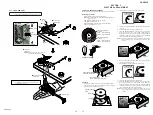
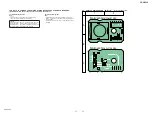
Sony PS-HX500 Service Manual Download Page 22

PS-HX500

PS-HX500

22

22

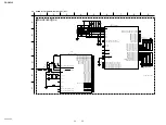
4-7.  SCHEMATIC  DIAGRAM - MAIN Section (4/4) -

R901
12K

R902
10K

R904

3.9K

R905

1K

C904
10u/25

IC901
TL431

JK901

5V /2A

R903

1K

C902
0.1u

C901
0.1u

L901

DXDA0708-01

POW

ER OFF

33

45

POW

ER OFF

33

45

SW901A

SW

SW901B

SW

W901

6P

Q903

2SC2712GR

Q904

RTR030P02

R906
10K

IC902
TPS61085DGK

C905
10u/25

C906

1u

L906

6.8uH/2A

D901
SM220B

R909
154K

R908
18K

R907
27K

C909
2200P

C908
0.1u

C910
10u/25

C911
10u/25

C918

470u/16

C917
0.1u

C912

10u/25

C907
10u/25

L908

FB(80)

C920

0.1u

IC903

TPS54232

C924

10u/25

C922
0.1u

R911

10K 

R912
47K

R910

820

C926
12P

C925
270P

C919
10u/25

D902
SM5819A

L907

10uH/1.84A

C923
0.1u

C929

0.47uF

C921
4.7u/25

L903

IC905

C930

100u/16u

C932

C933
0.1u

L904

FB(80)

C935
0.1u

IC904

C913

100u/16

C915

C914
0.1u

C916
0.1u

C934

Q911

C124EKA

C936
10u/25v

R915
18K

Q909
NC

Q910
NC

R913

NC

R914
NC

Q912

NC

R917

NC

R916

D903

1SS355

G

D

S

Q902

RRR030P03

R923
10K

Q901

C124EKA

C931
0.1u

C948

100u/10

POW

ER ON

POW

ER ON

CN901

6P

G

D

S

Q906

RRR030P03

R924

10K

Q905

C124EKA

L902

L905

C937

0.1u

C938

JR1
0

C942

22u

C903
0.1u

D905

SM4002

V0.2:ADD D905

IC906

TPS650061RUK

R921

47.5K

C950

0.1u

IC907

TPS3805H33DCK

R930
100K

R929

390K

C946

10u/25

R922

475K

R925

475K

L909
2.2u

C951

10u

C952
22P

C940
10u/25

R920

47K

R919
100K

R918
470K

Q908

2SC2712GR

Q907
2SC2712GR

C941

10u/25

C939

10u

C955
NC

R927

976K

R926

255K

A

A

A

P

L912

FB(80)

L910

FB(80)

C944
0.1u

C945

100u/10

C954

0.1u

C953

100u/10

C949
0.1u

L911

FB(80)

C943
NC

C947
NC

5V

PO

WO

N

33PLAY

12V

GND

V04:MODIFY:PS-HX500USBAUDIO04

PS-HX500OSCTAGO03
PS-HX500DSPPOWER02

FIXED1

FIXED2

CHASSIS

PGND

PGND

PGND

PGND

PGND

PGND

PGND

M

MOTOR

*

CHASSIS

R931

47K

Q914

C124EKA

R932

47K

GND

Q913

2SA1037AK

C956

0.1u

12V

-10.5V

FB(80)

NJM79M08DL1A

100u/16

BA08FP

100u/16

AP8V

A8V

100u/16

4.7K

AP-8V

5V

FB(80)

100u/16

A-8V

D3.3V

D1.2V

D3.3V

D1.2V

5V

D1.8V

R933
1K

R937

10 1/6 W

R936

10 

1
2
3

1

6

3

4

C1

2

3

4

5

G

0

G

0

C2

6

7

8

9

1

2

3

4

5

6

G

1

S

2

D

3

IN

6

EN

3

FREQ

7

GND

4

SS

8

COMP

1

FB

2

SW

5

1

2

BOOT

1

VIN

2

EN

3

SS

4

VSNS

5

COMP

6

GND

7

PH

8

Vin

2

G

1

OUT

3

IN

1

G

2

OUT

3

G

1

S

2

D

3

1

3

2

1

2

3

4

5

6

1

3

2

MR

1

TRST

2

EN_LDO1

3

EN_LDO2

4

PG

5

PGND

6

SW

7

VINDCDC

8

MODE

9

EN_DCDC

10

FB_DCDC

11

AGND

12

FB_LDO1

13

VLDO1

14

VINLDO1

15

FB-LDO2

16

VLDO2

17

VINLDO2

18

RSTSNS

19

RST

20

GND

21

NC

1

GND

2

RESET

3

VDD

4

SENSE

5

1

2

G

0

G

1

G

3

G

2

G

0

G

1

G

3

G

2

-

1

+

2

A

3

B

4

REST

FB(80)

(4/4)

MAIN BOARD

SW BOARD

A

3

8

6

E

2

9

D

5

B

C

7

1

4

F

Summary of Contents for PS-HX500

Page 1: ...r supply DC 5 V 2 0 A AC adaptor Power consumption 3 W Dimensions 430 x 104 x 366 mm 16 7 8 x 4 1 8 x 14 3 8 in width height depth Weight Approx 5 4 kg 11 9 lb 19 5 oz AC adaptor HK AR 050A200 US for the U S A and Canada Input AC 100 240 V 0 35 A 50 60 Hz Output DC 5 V 2 0 A HK AR 050A200 EU for European countries Input AC 100 240 V 0 35 A 50 60 Hz Output DC 5 V 2 0 A HK AR 050A200 GB for United K...

Page 2: ...made c omputer on a c omputer with a user upgraded operating system on a multi boo t computer with the power saving features of the computer System Suspend or Sleep Standby Trademarks IBM and PC AT are registered trademarks of International Business Machines Corporation Microsoft Windows and Windows Media are either trademarks or registered trademarks of Microsoft Corporation in the United States ...

Page 3: ...ary solder It is best to use only unleaded solder but unleaded solder may also be added to ordinary solder DESTINATION ABBREVIATIONS The following abbreviations for model destinations are used in this service manual Abbreviation CND Canadian model MODEL IDENTIFICATION Distinguish by Part No and Destination code of model number label stuck on the rear side of a main unit Rear Panel MODEL NUMBER LAB...

Page 4: ... the adhesive tape pull and hold the red ribbon and then hook the drive belt around the motor pulley Note Ş Do not twist the drive belt Ş Be sure to remove it once you have hooked the drive belt around the motor pulley 4 Place the rubber mat onto the platter Note Make sure that the chamfered side of the rubber mat faces upward The back side of the rubber is indicated by the SONY imprint REPLACING ...

Page 5: ...hands off to see if the tone arm is horizontally balanced Note Keep the tip of the stylus untouched with the rubber mat or the platter while adjusting the tone arm balance 6 Put the tone arm back onto the tone arm rest ADJUSTING THE STYLUS PRES SURE AND THE ANTI SKATING FORCE Once the tone arm is horizontally balanced adjust the stylus pressure and the anti skating force 1 Rotate only the gauge ri...

Page 6: ...MEMO PS HX500 6 ...

Page 7: ...S HX500 7 SPEED ADJUSTMENT SHEET STROBOSCOPE Used in electrical adjustment refer to page 15 Please enlarge to become diameter 292 mm It will be 292 mm in the 200 enlarge Please adjust if necessary 292 mm ...

Page 8: ...MEMO PS HX500 8 ...

Page 9: ... 7 FOOT ASSY COVER_MOTOR Page 12 2 11 TONE ARM ASSY Page 15 2 5 CASE Page 11 2 6 MAIN BOARD Page 11 2 9 MOTOR ASSY M1 Page 13 2 8 SWITCH KNOB Page 12 2 10 SW BOARD Page 14 SET STYLUS Note Illustration of disassembly is omitted Refer to REPLACING THE STYLUS on page 4 1 Fully open the dust cover 3 Remove the dust cover block in the direction of the arrow 5 hinge assy 5 hinge assy 6 dust cover assy 2...

Page 10: ...5 top side 3 Insert the your finger into the hole and remove the platter block in the direction of the arrow pulley belt 2 Remove the belt from the pulley hole hole 5 belt 6 platter top side 4 platter block Note 2 When installing the platter block refer to ASSEMBLING THE TURNTABLE on page 4 1 rubber mat Note 1 Make sure that the chamfered side of the rubber mat faces upward The back side of the ru...

Page 11: ... M3 u 8 9 screw M2 u 6 3 two screws 3 u 12 4 wire 5 two screws JTB3 u 15 6 Remove the MAIN board block in the direction of the arrow 7 pedestal 0 screw B M3 u 8 qa cover_rear qs MAIN board front side bottom side 7 pedestal front side rear side Note When turning the main unit over refer to NOTE IN THE CASE OF THE REVERSING THE MAIN UNIT on page 3 Note When turning the main unit over refer to NOTE I...

Page 12: ...tch knob When installing the switch knob to the rotary encoder align the directions of the D shaped tip of the rotary encoder and the D shaped notch at the inner side of the switch knob rotary encoder 2 switch knob switch knob front side bottom side front side top side Note 1 When turning the main unit over refer to NOTE IN THE CASE OF THE REVERSING THE MAIN UNIT on page 3 Note When turning the ma...

Page 13: ...top side Note 3 Removing the two screws is not necessary Note 3 Removing the screw is not necessary Note 4 If you remove the three screws step 2 the motor assy will fall When removing the screws make sure that you hold the motor assy Note 1 When turning the main unit over refer to NOTE IN THE CASE OF THE REVERSING THE MAIN UNIT on page 3 Note 2 When replacing the motor assy refer to DC MOTOR SPEED...

Page 14: ...k 5 pin Press the wire into the groove Press the wire into the groove CN901 front side bottom side front side 1 Remove the four solders 6 SW board 2 connector CN901 3 Draw the wire out of the groove 4 accessory nut 5 accessory washer Note When turning the main unit over refer to NOTE IN THE CASE OF THE REVERSING THE MAIN UNIT on page 3 ...

Page 15: ...unit by referring to Installation method 2 Place the rubber mat onto the turntable and place the speed adjustment sheet stroboscope onto it Rubber mat Turntable Speed adjustment sheet 3 The turntable is rotated at a rotation speed 33 rpm SPEED POWER rotary switch knob 4 Connect the socket fitted with a LED light bulb into an electri cal outlet 5 The LED light bulb is lit near to the turntable 6 In...

Page 16: ...PS HX500 PS HX500 16 16 SECTION 4 DIAGRAMS 4 1 BLOCK DIAGRAM ORFN ...

Page 17: ...r Side Parts face side Component Side Parts on the pattern face side seen from the pattern face are indicated Parts on the parts face side seen from the parts face are indicated For Schematic Diagrams Note All capacitors are in μF unless otherwise noted p pF 50 WV or less are not indicated except for electrolytics and tantalums All resistors are in Ω and 1 4 W or less unless otherwise specified 4 ...

Page 18: ...PS HX500 PS HX500 18 18 4 3 PRINTED WIRING BOARD MAIN Board Uses unleaded solder MAIN BOARD COMPONENT SIDE MAIN BOARD CONDUCTOR SIDE A B C D E F G H I J 1 2 3 4 5 6 7 8 9 K ...

Page 19: ...APWM0 GP8 7 MII_TXD 0 CLKS0 F3 SPI1_SCS 1 EPWM1A PRU0_R30 8 GP2 15 TM64P2_IN12 F18 SPI0_SCS 5 UART0_RXD GP8 4 MII_RXD 3 C19 SPI0_SCS 4 UART0_TXD GP8 3 MII_RXD 2 D18 SP10_SCS 3 UART0_CTS GP8 2 MII_RXD 1 SATA_MP_SWI TCH E17 SP10_SCS 2 UART0_RTS GP8 1 MII_RXD 0 SATA_CP_DE T D16 SP10_SCS 1 TM64P0_OUT12 GP 7 MDIO_CLK TM64P0_IN12 E16 SP10_SCS 0 TM64P1_OUT12 GP 6 MDIO_D TM64P1_IN12 D17 SP10_CLK EPWM0A GP...

Page 20: ...A_D 0 GP4 8 C9 PRU0_R30 5 GP2 7 PRU0_R31 15 B7 EMA_CS 5 GP3 12 B16 EMA_CS 4 GP3 13 F9 EMA_CS 2 GP3 15 B17 EMA_CS 0 GP2 0 A18 EMA_A_RW GP3 9 D10 EMA_OE GP3 10 B15 EMA_WE GP3 11 B9 PRU0_R30 1 GP2 1 PRU0_R31 1 B19 PRU0_R30 0 GP3 8 PRU0_R31 0 B18 EMA_CS 3 GP3 14 A17 TMS L16 TRST L17 TDI M16 TDO J18 TCK J15 GP8 0 K17 EMU1 K16 EMU0 J16 UART1_RxD SATA_LED GP1 1 E18 UART1_TxD SATA_CP_POD GP1 0 F19 USB1_DM...

Page 21: ...DD3318_B F7 DVDD3318_B F8 DVDD3318_B F10 DVDD3318_B F11 DVDD3318_B F12 DVDD3318_B F13 DVDD3318_B G9 DVDD3318_B J14 DVDD3318_B K15 DVDD3318_A F5 DVDD3318_A F15 DVDD3318_A G5 DVDD3318_A G14 DVDD3318_A G15 DVDD3318_A H5 DVDD18 F14 DVDD18 G6 DVDD18 G10 DVDD18 G11 DVDD18 G12 DVDD18 J13 DVDD18 K5 DVDD18 L6 DVDD18 P13 DVDD18 R13 VSS L9 P4 D1 2V D1 2V D1 8V D3 3V D1 8V D1 2V P5 P6 D1 2V D1 8V D3 3V D3 3V ...

Page 22: ...5K C950 0 1u IC907 TPS3805H33DCK R930 100K R929 390K C946 10u 25 R922 475K R925 475K L909 2 2u C951 10u C952 22P C940 10u 25 R920 47K R919 100K R918 470K Q908 2SC2712GR Q907 2SC2712GR C941 10u 25 C939 10u C955 NC R927 976K R926 255K A A A P L912 FB 80 L910 FB 80 C944 0 1u C945 100u 10 C954 0 1u C953 100u 10 C949 0 1u L911 FB 80 C943 NC C947 NC 5V POWON 33PLAY 12V GND V04 MODIFY PS HX500USBAUDIO04 ...

Page 23: ...ews are not sup plied Color Indication of Appearance Parts Ex ample KNOB BALANCE WHITE RED Parts Color Cabinet s Color 5 1 OVERALL SECTION 1 cabinet section 2 3 4 5 6 6 7 8 1 9 885 117 87 BELT Drive belt 2 9 885 209 94 PLATTER 3 9 885 209 95 RUBBER MAT PACKING ASSY Rubber mat 4 9 885 117 84 45 RPM ADAPTER 5 9 885 209 98 DUST COVER ASSY Including Rubbers Dust cover 6 9 885 209 99 HINGE ASSY Dust co...

Page 24: ...ge 51 9 885 210 18 SCREW 3X12 52 9 885 210 06 SPINDLE ASSY 53 9 885 210 03 FOOT ASSY 54 9 885 210 21 SCREW M2 5X1 5 STEP 55 9 885 210 20 SCREW 3X5 BTB 56 9 885 210 14 SCREW M3X8 B 57 9 885 210 13 SCREW 3X8 TTB 58 9 885 210 17 SCREW M2X6 59 9 885 210 07 MAIN BOARD COMPLETE 60 9 885 210 19 SCREW 3X15 JTB 61 9 885 210 08 SW BOARD COMPLETE Including Nut Washer Wire 62 9 885 210 02 SWITCH KNOB SPEED PO...

Page 25: ...ER 0 508 9 885 210 09 AC ADAPTOR UC HK AR 050A200 US US CND 0 508 9 885 210 10 AC ADAPTOR CEL HK AR 050A200 EU AEP 0 508 9 885 210 11 AC ADAPTOR CEK HK AR 050A200 GB UK 509 9 885 209 97 PHONO CABLE PHONO cables with grounding wires 510 9 885 209 96 USB CABLE 2 m The components identified by mark 0 or dotted line with mark 0 are critical for safety Replace only with part number specified Les compos...

Page 26: ...PS HX500 REVISION HISTORY Ver Date Description of Revision 1 0 2016 03 New ...

Reviews: