— 6 —
7
‘
’
4
MASTER INSERT (Tip: output, Ring:
input, Sleeve: GND)
These are input/output terminals for MASTER
OUTPUT. An external equipment can be inserted
before master volume.
5
EMG input terminals
This terminal receives signal from the emergency
broadcast facilities and makes this unit be in standby.
In this case, the EMG indicator on the front panel
lights up.
Select one of following two ways of connection as
follows.
When using the BREAK CONTACT terminal
Remove the short bar and connect the Relay of the
emergency broadcast facilities. When the relay is
contact is breaked, all AUDIO outputs of this unit will
be cut off.
When using the +24V IN terminal
This terminal receives signals of DC24V from the
emergency broadcast facilities.
When DC24V is cut off, all AUDIO outputs of this
unit will be cut off.
8
MIC input terminals (1:GND 2:HOT
3:COLD)
This is the input terminals for microphones.
In MIC1 and MIC2, wireless microphone has priority
while the tuner unit is used. (Refer to page 4
4
.)
9
+48V button
It supplies the Phantom power (DC+48V) to the MIC
1 - 4 terminals for condenser microphones.
When it is ON, DC+48V is output for the MIC
terminals except for the MIC4 on the front panel.
Notes
• Make sure to turn the MIC fader toward minimum before
connecting or disconnecting any cable or turning the +48
button to ON.
• Make sure to connect a line equipment to ST1 to ST3 inputs.
• When using a microphone powered by +48V and a dynamic
microphone simultaneously, the dynamic microphone may
not show its performance to the full.
6
CIRCUIT BREAKER
When over-current flows into the unit, the circuit
breaker cuts the power. In this case, remove the cause
of over-current and reset the breaker by pressing
RESET button.
7
SPEAKER output terminals
Connect with the speakers. C of the speaker
to the red terminal and - to the black terminal. Use
the speaker of 4 to 16 impedance.
0
ST1/ST2 input terminals
Use them for inputs from audio equipment.
Connect a playback equipment mainly to ST1 and a
record player to ST2.
!¡
ST3 (AV) input terminals
Use them for inputs from AV equipment.
Each of input A to D is selected by the SELECT
button on the front panel.
!™
MASTER OUTPUT terminals
Signal routed through the Master Volume are output
here.
!£
REC OUTPUT terminals
Signal not routed through the tone control (BASS,
TREBLE), BALANCE and Master Volume are output
here.
Video signal is the same as for MASTER OUT signal.
Remove the short bar of the
BREAK CONTACT terminal
BREAK
CONTACT
Relay
‘
’
‘
’
or
(+24V output)
The emergency broadcast facilities
(+ 24V IN)
8
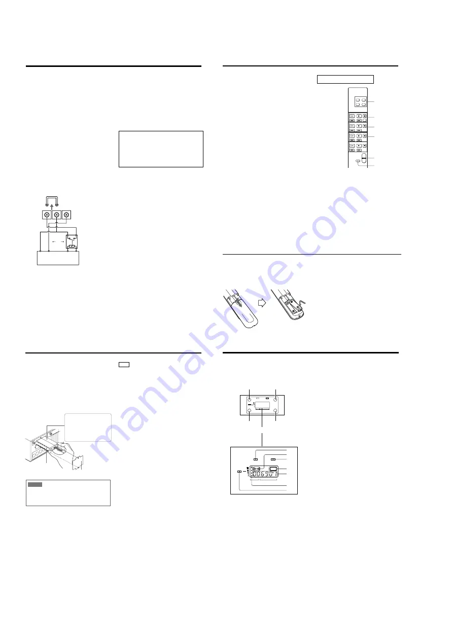
Remote control
1
FUNCTION button
Use to select one of ST3 A to D input.
2
CD deck operation buttons
Use to operate the Sony CD deck.
3
MD deck operation buttons
Use to operate the Sony MD deck.
4
TAPE deck operation buttons (A, B)
Use to operate the Sony TAPE deck.
5
MASTER VOLUME operation knob
Use to adjust the master volume level.
6
MUTING button
Use to mute the output signal from MASTER OUT-
PUT, MASTER INSERT, ECHO SEND, MIC
GROUP OUTPUT or SPEAKER output terminals.
!¢
ECHO SEND/RETURN terminals
Connect effectors such as reverbrators and delay units
to this terminal.
SEND terminal
This terminal outputs audio signals mixed by ECHO/
AUX SEND knob of MIC1 to MIC4 and ST1 to ST3
in monaural
RETURN terminals
This is an input terminal for signal returned from the
effector. When the ECHO RETURN switch on the
front panel is set to ON, these are assigned to L and to
R.
Adjust the input level using effector's level controller.
!∞
MIC GROUP and ASSIGN switch
MIC GROUP OUTPUT terminal
It outputs signal of which level is adjusted by MIC
GROUP knob.
ASSIGN switch
This is normally on.
When this switch is set to OFF, the microphone signal
for MASTER OUTPUT and SPEAKER terminals are
cut off.
Using this, turn it OFF when a PA system with ceiling
speakers and external power amplifier.
INSERT terminal (Tip: output, Ring: input, Sleeve:
GND)
Use it to connect an external graphic equalizer or a
feedback reducer.
!§
MODE switch
It will be monaural when MASTER INSERT, MAS-
TER OUTPUT and SPEAKER output are set to
MONO.
!¶
POWER cord
Inserting batteries into the remote
A
B
C
CD
DISC SKIP
MUTING
MD
TAPE DECK A
TAPE DECK B
MASTER
VOLUME
D
1
2
3
4
5
6
You can control this unit with using the supplied remote.
Insert two R6 (size AA) batteries by matching the + and –
on the batteries. When using the remote, point it at the
remote sensor on the equipment.
When to replace batteries
With normal use, the batteries should last for about six
months. When the remote no longer operates the equip-
ment, replace all the batteries with new ones.
Notes
• Do not leave the remote near an extremely hot or humid
place.
• Do not drop any foreign object into the remote casing,
particularly when replacing the batteries.
• Do not expose the remote sensor to direct sunlight or lighting
apparatuses. Doing so may cause a malfunction.
• If you don't use the remote for an extended period of time,
remove the batteries to avoid possible damage from battery
leakage and corrosion.
Location and Function of Parts
9
Tuner unit
Tuner cover
Installation of The Tuner Unit
1
Turn off the power of this unit.
2
Remove the tuner cover.
3
Check the up and down sides of the tuner unit, and
insert it into the slot.
The upper slot corresponds to MIC1 and the lower slot
to MIC2. (Set the group and channel of the tuner unit
to same as wireless microphone's one.)
NOTICE
To prevent breakdown or injury, do not put your hand
inside of the slot except when you install or remove the
tuner unit.
Insert it deeply into the compart-
ment.
Do not insert or remove the tuner
unit while the power is on. This
may be cause of noise or
malfunction of the connector.
4
Fix the tuner cover.
After installation of the tuner unit, turn on the power
of the unit and turn on the power of the wireless
microphone to check it is receiving. While receiving,
the RF/SIGNAL indicator lights up. Note that the
RF/SIGNAL indicator will not light up when the
setting channel of the microphone is different from
the setting of the tuner unit, or when the microphone
power is consumed.
Notes
Take the following precautions to prevent interference
and noise.
• If there is a TV broadcasting station nearby, to avoid
possible interference from its broadcasting, do not
use that station's channel.
• When simultaneously using two tuners, always set
the tuners to different channels within the same group
(other than group 00).
• Please make a choice of model in accordance with
your area to use picking up an unused TV channel.
• Make sure that the channel selected on the micro-
phone is the same as that selected on the tuner being
used in the same system.
10
RF
AF
DISPLAY
GP
CH
BATT
GP
AF
GP
CH
BATT
CH
+
_
RF
1
1
3
2
4
2
3
4
5
7
6
1
AF (audio frequency) indicator
2
AF (audio frequency) level indications
The indicator lights and the indications appear when
the audio output level is higher than the reference
level.
3
BATT (battery) indicator
4
BATT (battery) indication
Indicate the condition of the wireless microphone
transmitter batteries. The indicator and indication
appear and start flashing about one hour before the
transmitter batteries go flat.
The time at which flashing begins will depend on the
type of battery used in the transmitter, and its
condition.
5
GP/CH (group/channel) indication
Shows the reception channel group and respective
channel number.
Pressing the + button changes this indication to the
frequency indication.
6
RF (ratio frequency) level indications
7
RF (ratio frequency) indicator
The indicator lights and the indications (dots) appear
when the antenna reception is optimal. Depending on
the RF input level, the number of dots changes.
Please refer to the table Sony 800MHz-band system models frequency range in the Operating Manual of Wireless Micro-
phone or Transmitter.
1
GP (group) button
To change the group, press the + or – button while
holding this button down.
2
CH (channel) button
To change the channel in a group, press the + or –
button while holding this button down.
3
+ button
To go to a higher group or channel, press this button
while holding the GP or CH button.
Press this button changes the indication from GP/CH
to frequency.
4
– button
To go to a lower group or channel, press this button
while holding the GP or CH button.