
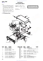
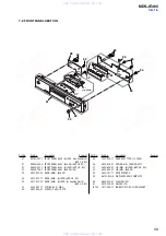
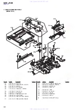
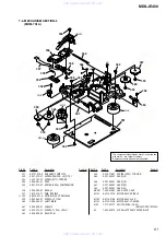
49
MDS-JE480
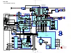
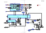
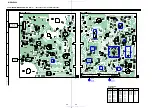
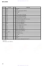
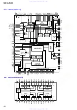
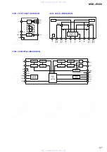
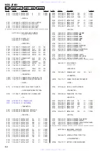
6-13. IC PIN FUNCTION DESCRIPTION
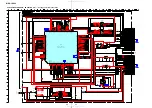
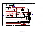
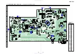
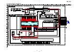
• IC101 CXA2523AR RF Amplifier (BD BOARD)
Pin No.
Pin Name
I/O
Description
I
J
VC
A to F
PD
APC
APCREF
GND
TEMPI
TEMPR
SWDT
SCLK
XLAT
XSTBY
F0CNT
VREF
EQADJ
3TADJ
Vcc
WBLADJ
TE
CSLED
SE
ADFM
ADIN
ADAGC
ADFG
AUX
FE
ABCD
BOTM
RFO
MORFI
MORFO
I
I
O
I
I
O
I
—
I
O
I
I
I
I
I
O
I
I
—
I
O
—
O
O
I
—
O
O
O
O
O
O
O
—
I
O
I
—
O
I
O
I
O
I-V converted RF signal I input
I-V converted RF signal J input
Middle point voltage generation output
Signal input from the optical pick-up detector
Light amount monitor input
Laser APC output
Reference voltage input for setting laser power
Ground
Temperature sensor connection
Reference voltage output for the temperature sensor
Serial data input from the CXD2664R
Serial clock input from the CXD2664R
Latch signal input from the CXD2664R
“L”: Latch
Stand by signal input
“L”: Stand by
Center frequency control voltage input of BPF22, BPF3T, EQ from the CXD2664R
Reference voltage output (Not used)
Center frequency setting pin for the internal circuit EQ
Center frequency setting pin for the internal circuit BPF3T
Power supply
Center frequency setting pin for the internal circuit BPF22
Tracking error signal output to the CXD2664R
External capacitor connection pin for the sled error signal LPF
Sled error signal output to the CXD2664R
FM signal output of ADIP
ADIP signal comparator input
ADFM is connected with AC coupling
External capacitor connection pin for AGC of ADIP
ADIP duplex signal output to the CXD2664R
I
3
signal/temperature signal output to the CXD2664R
Focus error signal output to the CXD2664R
Light amount signal output to the CXD2664R
RF/ABCD bottom hold signal output to the CXD2664R
RF/ABCD peak hold signal output to the CXD2664R
RF equalizer output to the CXD2664R
External capacitor connection pin for the RF AGC circuit
Input to the RF AGC circuit
The RF amplifier output is input with AC coupling
User comparator output (Not used)
User comparator input (Fixed at “L”)
External capacitor pin for cutting the low band of the ADIP amplifier
User operation amplifier output (Not used)
User operation amplifier inversion input (Fixed at “L”)
RF amplifier output
Groove RF signal is input with AC coupling
Groove RF signal output
1
2
3
4 - 9
10
11
12
13
14
15
16
17
18
19
20
21
22
23
24
25
26
27
28
29
30
31
32
33
34
35
36
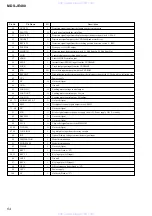
46
47
48
• Abbreviation
APC: Auto Power Control
AGC: Auto Gain Control
www. xiaoyu163. com
QQ 376315150
9
9
2
8
9
4
2
9
8
TEL 13942296513
9
9
2
8
9
4
2
9
8
0
5
1
5
1
3
6
7
3
Q
Q
TEL 13942296513 QQ 376315150 892498299
TEL 13942296513 QQ 376315150 892498299


