background image

10

ICD-BM1/BM1PRO

Note :

 This set can be disassemble according to the following sequence.

SECTION 2

DISASSEMBLY

Note :

 Follow the disassembly procedure in the numerical order given.

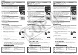
2-1. KNOB (REAR)

2-1.

KNOB (REAR)
(Page 10)

2-2.

CHASSIS BLOCK ASSY
(Page 11)

SET

2-3.

SW BOARD
(Page 11)

2-4.

PLATE (MS) SECTION
(Page 12)

2-5.

LCD BOARD
(Page 12)

2-6.

CHASSIS SECTION
(Page 13)

2-7.

MEMORY STICK CONNECTOR
(Page 13)

2-8.

MAIN BOARD
(Page 14)

5

 precision pan screw

    (M1.4) (EG)

6

 precision pan screw

    (M1.4) (EG)

2

 two knobs (rear)

3

 pullout the lid connector.

4

 lid (connector)

1

1

Ver. 1.1

Summary of Contents for ICDBM1 - Memory Stick Media Digital Voice Recorder

Page 1: ...ural sound LP Long play recording mode monaural sound Frequency range ST 60 Hz 13 500 Hz SP 60 Hz 7 000 Hz LP 80 Hz 3 500 Hz Speaker approx 28 mm 29 32 in dia Power output 350 mW Input Output Earphone jack minijack for 8 300 ohms ear receiver headphones Microphone jack minijack stereo Plug in power Minimum input level 0 7 mV 3 kilohms or lower impedance microphone USB connector DC IN 3V jack Playb...

Page 2: ...ead Caution Some printed circuit boards may not come printed with the lead free mark due to their particular size LEAD FREE MARK Unleaded solder has the following characteristics Unleaded solder melts at a temperature about 40 C higher than ordinary solder Ordinary soldering irons can be used but the iron tip has to be applied to the solder joint for a slightly longer time Soldering irons using a ...

Page 3: ...supplied is connected the indicator does not appear 8 Alarm indicator 45 Appears when the alarm is set for a message 9 Recording mode indication 50 ST High quality recording mode stereo sound with an external stereo microphone not supplied SP Standard play recording mode monaural sound LP Long play recording mode monaural sound 0 Microphone sensitivity indication 17 Displays the current microphone...

Page 4: ...nit has been without battery for a certain period of time In this case proceed from step 4 1 Slide POWER to ON The IC recorder is turned on 2 Press MENU The menu mode will be displayed in the display window 3 Press the jog lever up or down to select DATE TIME Press up Press down POWER MENU ENTER CANCEL 9GB Getting Started 4 Press ENTER The date and time setting window is displayed The year digits ...

Page 5: ...ll the folders and the maximum number of messagesare asfollows You can record messagesfor the maximum recording time in a single folder 4MB 8MB 16MB 32MB 64MB 128MB ST 10min 20min 40min 1hr 25min 2hr 50min 5hr 50min SP 30min 1hr 2hr 10min 4hr 20min 8hr 50min 17hr 45min LP 1hr 20min 2hr 50min 5hr 45min 11hr 45min 23hr 35min 47hr 25min Number 456 950 963 1 016 1 016 1 016 of Messages ST High quality...

Page 6: ...cording switch to ON during stop or recording mode Setthe control key to REC Recording starts when the unit detectssound and VOR appearsin the display window The recording pauseswhen no sound is detected and VOR PAUSE appears Notes Recording will not be started unless the control key is setto REC VOR function is affected by the sound around you Set the MIC SENS microphone sensitivity switch accord...

Page 7: ...eep and playback stops Move the control key to STOP 1 To listen from an ear receiver Connect the supplied ear receiver to the i headphones jack The built in speaker will be automatically disconnected 1 To listen from an external speaker Connect an active or passive speaker not supplied to the i headphones jack Note Playback after the overwrite recording starts from the beginning of the message Pla...

Page 8: ...s Erasing Messages You can erase the recorded messages one by one or all messages in a folder at a time Note Once a recording has been erased you cannot retrieve it Erasing Messages one by one Be sure to erase unnecessary messages only When a message is erased the remaining messages will advance and be renumbered so that there will be no space between messages ERASE FOLDER ENTER CANCEL Erase Messa...

Page 9: ... ENTER The formatting window will be displayed 4 Press the jog lever up or down to select YES Jog lever MENU ENTER CANCEL Continued 48GB Formatting a Memory Stick continued 5 Press ENTER OK will be displayed in the display window 6 Press ENTER again Formatting starts FORMATTING will be displayed on the display After formatting the display in step 2 will appear in the display window 7 Press MENU to...

Page 10: ...r given 2 1 KNOB REAR 2 1 KNOB REAR Page 10 2 2 CHASSIS BLOCK ASSY Page 11 SET 2 3 SW BOARD Page 11 2 4 PLATE MS SECTION Page 12 2 5 LCD BOARD Page 12 2 6 CHASSIS SECTION Page 13 2 7 MEMORY STICK CONNECTOR Page 13 2 8 MAIN BOARD Page 14 5 precision pan screw M1 4 EG 6 precision pan screw M1 4 EG 2 two knobs rear 3 pullout the lid connector 4 lid connector 1 1 Ver 1 1 ...

Page 11: ...screws 1 4 1 Open the shutter MS broken the switch 5 chassis block assy 4 2 Push the attachment battery lid about 5mm 4 screw 1 4 3 8 screw 1 4 3 9 screw 1 4 3 3 CN951 0 SW board 1 two claws 5 two claws qa ornament block assy 7 6 two claws 2 ornament MIC Ver 1 1 ...

Page 12: ...SECTION 2 5 LCD BOARD 3 screw 1 4 3 2 precision pan screw M1 4 EG 1 MIC301 4 claw 6 plate MS section 5 claw 1 screw self tap 4 2 claw 7 two claws 8 two claws 9 holder LCD qa EL901 qs LCD board 0 LCD901 3 CN902 5 CN903 6 CN901 Ver 1 1 ...

Page 13: ...13 ICD BM1 BM1PRO 2 6 CHASSIS SECTION 2 7 MEMORY STICK CONNECTOR 1 two claws 3 claw 2 claw 4 claw 5 6 CN701 7 chassis rear section 8 chassis front section 1 memory stick connector 2 chassis rear ...

Page 14: ...14 ICD BM1 BM1PRO 2 8 MAIN BOARD 1 Remove the soldering of speaker 5 claw 2 Remove the soldering of MIC301 3 MIC301 4 precision pan screw M1 4 EG 6 MAIN board chassis front ...

Page 15: ...ore power supply 1 5 V 25 HD7 I O Host data bus Not used 26 HD6 I O Host data bus Not used 27 GND GND 28 EVDD I O power supply 3 0 V 29 XHCS I Host chip select Pull up 30 HA1 I Host data access 1 Pull down 31 XHWR I Host write Pull up 32 HA0 I Host data access 0 Pull down 33 XHRD I Host read Pull up 34 TIMOUT O Not used 35 SO O Serial data output 36 XHWE O Host write enable Not used 37 XHRE O Host...

Page 16: ...ot used 79 EVDD I O power supply 3 0 V 80 MA17 O Memory address 17 Not used 81 to 84 NC Not used 85 EVDD I O power supply 3 0 V 86 MA18 O Memory address 18 Not used 87 MA19 O Memory address 19 Not used 88 XMHOLDAK O Memory bus hold response Not used 89 XMRD O Memory read out Not used 90 XMHOLDRQ I Memory bus hold request Pull up 91 GND GND 92 EVDD I O power supply 3 0 V 93 XMWAIT I Memory access w...

Page 17: ...133 CSTOP I Clear stop mode Pull down 134 IC Internal connection Not used 135 GND GND 136 and 137 PLL0 PLL1 I PLL rate setting 0 and 1 138 XRST I Reset 139 GND GND 140 IVDD Core power supply 1 5 V 141 PLL3 I PLL rate setting 3 142 HALTS O HALT 143 GND GND 144 and 145 IVDD Core power supply 1 5 V 146 PLL2 I PLL rate setting 2 147 GND GND 148 EVDD I O power supply 3 0 V 149 CLKOUT O Clock output 150...

Page 18: ...I F 23 SCK1 O Serial clock for RTC and EEPROM 24 SDO1 O Serial data output for RTC S P and EEPROM 25 XLCDRST O LCD reset 26 and 27 A15 A16 O SRAM address bus 28 CCVDD Core power supply 2 6 V 29 SIPCLK O Clock for S P 30 BEEP O Beep 31 DREQ I USB DMA request input 32 POWERSW I POWER switch detection 33 RTCCS O Chip select for RTC 34 XADACS O Chip select for A D D A converter 35 XDSPSIOEN O DSP I F ...

Page 19: ...KE0 KEY1 KEY2 I Key entry 0 1 and 2 89 VORDPC I VOR DPC switch detection 90 MICSENS I MIC SENS switch detection 91 BATTAD I Battery voltage detection 92 JACKDET I Microphone headphone jack detection 93 SDI1 I Serial data input for RTC and EEPROM 94 VREF I Reference voltage for A D 3 1 V 95 AVcc I Power supply for A D 3 1 V 96 to 98 MD0_MD2 I Mode pin 99 TEST I Test pin 100 CCVDD Core power supply ...

Page 20: ...20 ICD BM1 BM1PRO MEMO ...

Page 21: ...D CK Q J301 SPEAKER 2 3 4 1 6 3 9 7 10 IC705 EEPROM IC703 REAL TIME CLOCK SK DI DO CS RESET CLK DI CE XIRQ IC301 ADC DAC HEADPHONE AMP AINR2 AINL2 HPR HPL MOUT PDN STDO SDTI 6 MCLK SCKI 18 MIN CDTI CSN IC601 DSP IRIS ADASI 7 40 BICK BCLK 5 47 LRCK LRCK 150 CLKIN MCLK XRST TSO TSCK TSOEN 55 TSIEN 158 TSIOEN TSI REQ SDIO SCK0 XDSPSIOEN SDO0 DSPIFREQ MSDIO MSCLK MSBS MSINS DIO SCLK BS INS CF1 CF2 X70...

Page 22: ...VDD MEMORY STICK CCVDD IC701 PLUG IN POWER IVDD IC601 DC DC CONV 1 5 87 KEY1 S901 907 FUNCTION KEY 36 MSLOCK 88 KEY2 S956 958 MODE SWITCH WAKE UP DETECT 1 4 5 3 1V REG 1 3 5 IC509 3 1V REG IC502 4 3 IC508 2 4V REG 3 B LIGHT CIVDD IC701 DVDD IC301 CVDD IVDD IC801 LCD MODULE IC504 5 4 3 IC501 1 6V DC DC CONV 2 1 VOLTAGE DETECT Q504 B SWITCH 5 3 1 CE FB EXT XLIGHT VDD EL Q503 3 1 IC503 DRY BATTERY 3V...

Page 23: ...possible to measure Voltages are taken with a VOM Input impedance 10 MΩ Voltage variations may be noted due to normal produc tion tolerances Waveforms are taken with a oscilloscope Voltage variations may be noted due to normal produc tion tolerances Circled numbers refer to waveforms Signal path F PB L REC IC601 IC702 on main board are not replaceable The voltages and Waveform of CSP chip size pac...

Page 24: ...01 D503 C506 L501 L502 C737 R707 R708 JC701 Q511 R722 R760 CN701 C303 TP701 TP702 TP707 TP511 TP706 TP705 TP505 TP503 TP801 J501 DC IN 3V J301 i J302 m PLUG IN POWER TP501 TP802 TP803 TP502 SP301 SPEAKER DRY BATTERY SIZE AAA IEC DESIGNATION LR03 2PCS 3V CSP CHIP SIZE PACKAGE CSP CHIP SIZE PACKAGE TP301 TP302 TP507 TP508 TP709 CL613 CL607 CL608 IC601 CL612 CL610 CL713 CL609 CL611 CL606 CL604 CL605 ...

Page 25: ...17 C318 R321 R322 C315 C316 C314 IC301 C301 R513 C313 C311 IC801 R812 R813 C806 R810 C807 C801 0802 R814 R818 R819 C803 R816 R817 R804 R807 FB801 R734 C721 C720 D702 TP787 TP788 C728 IC703 IC704 C733 R756 IC705 C809 IC505 MIC301 TP101 IC303 SP301 FB302 R317 C212 C112 C320 C804 X801 C805 R808 CN801 FB802 R720 R755 R309 R750 Q301 Refer to page 23 for Common Note on Schematic Diagrams and Waveform 3 ...

Page 26: ...18 CL713 IC707 C708 C707 X701 C729 C727 R753 R726 IC706 C735 R730 R725 R724 C702 C703 C704 C705 CN702 RB701 TP703 TP514 TP704 TP705 TP706 C737 CN701 Q702 IC702 Q704 R319 Q703 Q701 C719 C722 IC701 R758 R701 JC701 R707 R708 R760 C716 3 6 SCHEMATIC DIAGRAM MAIN SECTION 2 3 Refer to page 23 for Common Note on Schematic Diagrams and Waveform Page 27 Page 25 Page 28 Ver 1 1 ...

Page 27: ... R507 R509 C513 TP511 R521 R517 C525 TP505 IC506 IC509 C532 C518 C529 C528 C533 C531 C521 C520 IC513 R622 R614 R523 RB603 IC601 RB602 IC602 R621 X601 C603 C606 CL609 RB604 C602 C601 RB605 C608 R704 R705 CL604 CL605 CL606 RB606 CL607 C605 CL608 D801 R604 R605 Q501 Q509 Q504 Q505 Q506 Q507 TH501 Q502 IC502 Q503 Q511 C523 IC501 IC503 IC508 RB601 R613 C607 C512 D506 3 7 SCHEMATIC DIAGRAM MAIN SECTION ...

Page 28: ...S904 S905 S906 S907 S908 TP902 TP903 IC901 R901 C915 R906 C901 C902 C903 C904 C905 C906 C907 C908 C909 R904 R905 R907 R909 CN901 R908 CN903 CN951 D951 R968 R973 C951 R951 R952 C954 S954 S957 S959 S960 S962 R972 R970 R969 R966 R963 R962 R964 R965 S956 S958 R958 R957 R953 R956 R959 RB951 CN902 Q951 S961 S955 Q952 S952 S951 S953 C910 C913 C914 C953 C952 D952 R974 EL901 Page 26 Ver 1 1 ...

Page 29: ...1 1 19 R907 R908 R909 R905 R904 C908 C907 C906 C909 R918 R916 R917 C913 R914 IC901 LCD901 EL BACK LIGHT EL901 4 3 22 1 1 2 R913 C914 R911 R920 R912 R915 ERASE S908 CANCEL S901 ENTER S906 11 1 860 924 11 1 860 924 FOLDER S904 DISPLAY S902 MENU S903 PRIORITY S905 DIVIDE S907 D901 TP903 TP902 3 9 PRINTED WIRING BOARD LCD SECTION Refer to page 23 for Common Note on Printed Wiring Boards Uses unleaded ...

Page 30: ...R956 C952 C951 R973 R953 C954 RB951 C953 D952 R974 R968 R951 R962 S957 S954 VOL R963 R959 R966 R952 CN951 1 5 10 14 11 1860 923 11 1 860 923 Q951 Q952 S960 S959 S962 NEW FILE D951 OPR SW BOARD SIDE A SW BOARD SIDE B S956 FUNCTION A S958 FUNCTION B S956 958 FUNCTION REC STOP PLAY B SPACE 3 10 PRINTED WIRING BOARD SW SECTION Refer to page 23 for Common Note on Printed Wiring Boards Uses unleaded sol...

Page 31: ...HVSS HVDD HPR AINL1 AINR1 AINL2 AINR2 AVDD AVSS VCOM VREF LIN RIN MIN MOUT MUTET HPL IPGA ADC DAC ADC DAC HPF DATT VCOM VREF BOOST IPGA AINL1 AINL2 AINR1 AINR2 1 2 3 4 VDD FOE XIRQ T1 5 10 9 8 7 6 FOUT CE CLK DO DI CE CLK DO DI CE CLK DO DI GND FOUT CONTROLLER DIVIDER OSC 32 768kHz INTERRUPTS CONTROLLER BUS INTERFACE CIRCUIT CONTROL REGISTER AND SYSTEM CONTROLLER TIMER REGISTER CLOCK AND CALENDAR ...

Page 32: ... SPAMP XSTMIC XREDLED XGRLED 4 XLIGHT1 CLK DATA VSS OUTPUT BUFFER OPEN DRAIN IC704 BU2090FS E2 MAIN Board 1 3 IC705 AK6417CH E2 MAIN Board 1 3 EEPROM R W AMPS AND AUTO ERASE INSTRUCTION DECODE CONTROL AND CLOCK GENERATION INSTRUCTION REGISTER VCC RDY BUSY RESET GND CS SK DI DO ADD BUFFERS DATA REGISTER VPP GENERATOR DECODER VPP SW VREF 16 16 16384bit 1024 16 1 2 3 4 8 7 6 5 ...

Page 33: ...IVDD XOUT XIN CVDD GND A1 A2 A3 A4 A5 A6 D0 D1 D2 D3 D4 D5 D6 D7 D11 D10 D9 D8 IVDD GND D12 D13 D14 D15 A0 HWR BYTE INT0 RD LWR CS RST DREQ0 DACK0 I O BLOCK USB IP OSCILLATION BUFFER 48MHzPLL VBUS INPUT CIRCUIT D PIN PULLUP CIRCUIT USB TRANSCEIVER TRANSFER CONTROLLER SERIAL INTERFACE ENGINE SIE INTERRUPT CONTROLLER ENDPOINT CONTROLLER FIFO MEMORY CONTROLLER FIFO MEMORY BUS INTERFACE UNIT BIU IC801...

Page 34: ...ould be anticipated when ordering these items Color Indication of Appearance Parts Example KNOB BALANCE WHITE RED Parts Color Cabinet s Color Accessories are given in the last of this parts list R R 1 3 260 469 01 ATTACHMENT BATTERY LID 2 3 252 824 11 SCREW 1 4 3 3 260 472 01 HINGE BATTERY LID 4 3 260 475 02 LID BATTERY CASE 5 3 260 471 01 TERMINAL BATTERY 6 3 248 370 01 SCREW SELF TAP 7 3 260 459...

Page 35: ...ET SPEAKER 53 3 260 436 01 BUTTON VOL 54 3 260 461 01 WINDOW LCD 55 3 260 460 02 SHEET WINDOW ADHESIVE 56 3 260 506 01 SHEET ERASE ADHESIVE 57 3 260 435 01 BUTTON ERASE 58 3 261 295 01 BUTTON FRONT B 59 3 260 426 01 BUTTON FRONT A 60 3 260 498 01 SHEET CASE ADHESIVE 51 52 53 60 54 55 56 57 59 58 not supplied not supplied not supplied Ver 1 1 ...

Page 36: ...5 01 SPRING REVIEW TORSION 112 3 247 180 01 SCREW 1 4X3 113 3 225 996 12 SCREW M1 4 EG PRECISION PAN 114 3 260 488 01 FRAME MS 115 3 260 546 01 CUSHION MICROPHONE 116 3 260 482 01 PLATE MS 117 3 260 484 01 SHUTTER MS 118 3 260 483 01 SLIDER MS 119 3 264 960 01 LEAF SLIDE COPPER MIC301 1 542 572 11 MICROPHONE ELECTRET CAP Mic Ref No Part No Description Remark Ref No Part No Description Remark 101 1...

Page 37: ...CK 156 3 260 501 01 CUSHION EL 157 3 248 370 01 SCREW SELF TAP 158 A 4541 671 A LCD BOARD COMPLETE EL901 1 805 472 11 ELEMENT EL LCD901 1 477 070 11 INDICATOR UNIT LIQUID CRYSTAL SP301 1 825 645 11 SPEAKER 2 8cm Ref No Part No Description Remark Ref No Part No Description Remark LCD901 not supplied not supplied EL901 SP301 151 152 153 154 156 157 158 155 4 4 CHASSIS 1 SECTION ...

Page 38: ...01 CAP TERMINAL 206 3 260 491 01 CHASSIS FRONT 207 3 221 591 01 NUT M1 4 208 3 260 489 01 CHASSIS REAR 209 3 260 480 01 SHEET MS ADHESIVE 210 3 260 486 01 WINDOW MS 211 1 818 067 11 CONNECTOR MEMORY STICK 212 3 261 081 01 SHEET CONNECTOR Ref No Part No Description Remark Ref No Part No Description Remark 201 203 204 205 206 207 208 212 210 211 209 207 207 202 4 5 CHASSIS 2 SECTION ...

Page 39: ... 11 RES CHIP 47 5 1 16W R907 1 218 953 11 RES CHIP 1K 5 1 16W R908 1 218 985 11 RES CHIP 470K 5 1 16W R909 1 218 985 11 RES CHIP 470K 5 1 16W R911 1 218 953 11 RES CHIP 1K 5 1 16W R912 1 218 953 11 RES CHIP 1K 5 1 16W R913 1 218 957 11 RES CHIP 2 2K 5 1 16W R914 1 218 957 11 RES CHIP 2 2K 5 1 16W R915 1 218 961 11 RES CHIP 4 7K 5 1 16W R916 1 218 965 11 RES CHIP 10K 5 1 16W R917 1 218 969 11 RES C...

Page 40: ... CHIP 47uF 20 6 3V C721 1 125 777 11 CERAMIC CHIP 0 1uF 10 10V C722 1 125 777 11 CERAMIC CHIP 0 1uF 10 10V C727 1 125 777 11 CERAMIC CHIP 0 1uF 10 10V C728 1 125 777 11 CERAMIC CHIP 0 1uF 10 10V C729 1 125 777 11 CERAMIC CHIP 0 1uF 10 10V C733 1 125 777 11 CERAMIC CHIP 0 1uF 10 10V C735 1 125 777 11 CERAMIC CHIP 0 1uF 10 10V C737 1 125 777 11 CERAMIC CHIP 0 1uF 10 10V C738 1 125 777 11 CERAMIC CHI...

Page 41: ...0K 0 5 1 16W R506 1 218 989 11 METAL CHIP 1M 0 5 1 16W R507 1 218 989 11 METAL CHIP 1M 0 5 1 16W R508 1 218 989 11 METAL CHIP 1M 0 5 1 16W R509 1 220 804 11 RES CHIP 2 2M 5 1 16W R510 1 218 985 11 RES CHIP 470K 5 1 16W R512 1 218 985 11 RES CHIP 470K 5 1 16W R513 1 218 985 11 RES CHIP 470K 5 1 16W R514 1 216 809 11 METAL CHIP 100 5 1 10W R515 1 216 809 11 METAL CHIP 100 5 1 10W R516 1 218 977 11 R...

Page 42: ...18 953 11 RES CHIP 1K 5 1 16W R956 1 218 981 11 RES CHIP 220K 5 1 16W R957 1 218 961 11 RES CHIP 4 7K 5 1 16W R958 1 218 953 11 RES CHIP 1K 5 1 16W R959 1 218 977 11 RES CHIP 100K 5 1 16W R962 1 218 953 11 RES CHIP 1K 5 1 16W R963 1 218 953 11 RES CHIP 1K 5 1 16W R964 1 218 977 11 RES CHIP 100K 5 1 16W R965 1 218 981 11 RES CHIP 220K 5 1 16W R966 1 218 957 11 RES CHIP 2 2K 5 1 16W R968 1 218 989 1...

Page 43: ...43 ICD BM1 BM1PRO MEMO ...

Page 44: ...sion allows you to jump to the revised page Also clicking the version at the upper on the revised page allows you to jump to the next revised page Ver Date Description of Revision 1 0 2003 11 New 1 1 2007 04 Review of mechanism parts and electric parts ...

Reviews: