background image

HCD-SLK10D/SLK20D

HCD-SLK10D/SLK20D

50

50

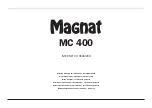
5-19.  SCHEMATIC  DIAGRAM - MAIN Section (1/4) -

• See page 56 for IC Block Diagrams.

BOARD

44

(4/4)

MAIN

BOARD

MAIN

42

(2/4)

BOARD

MAIN

43

(3/4)

MAIN

41

(4/4)

BOARD

IC B/D

CN611

K

TERMINAL

BOARD

CN614

M

TERMINAL

BOARD

CN613

J

TERMINAL

BOARD

CN612

L

TERMINAL

BOARD

14.7

14.7

14.7

0

14.7

14.7

14.7

14.7

14.7

0

0

0

3.3

0

1.1

3.5

3.3

1.6

1.6

1

1.7

1.6

1.6

1.7

3.3

3.3

3.3

0

3.3

3.3

1.7

0

12.3

26.1

14.7

29.4

29.4

14.7

12.3

12.3

1.1

12.3

12.3

26.1

14.7

14.7

29.4

29.4

14.7

29.4

26.1

29.4

14.7

14.7

29.4

26.1

29.4

14.7

0.5

0.5

0

12.3

6.3

0

0.6

0.5

0

3.3

11.7

11.7

0.6

0

5.7

7

0

R606

JL670

JL669

47k

R655

50V

10

C635

10k

R673

3.3

R555

JL563

3.3

R526

2.2

C532

100k

R670

JL514

0

R671

0

R572

100k

R668

1

C588

10uH

L588

2.2

C542

0

R521

JL671

100

R502

3.3

R664

100k

R672

4700p

C503

0.033

C541

3.3

R556

100

R515

100k

R669

JL664

1

C578

10

C649

JL513

3.3

R663

10uH

L578

3.3

R525

JL665

2.2

C549

0.033

C554

2.2

C539

R570

0

0

R564

0

R608

0

R609

0

R611

0

R607

0

R512

PWM3_LI

PWM3_LD

PWM3_RI

PWM3_RD

100p

C502

3.3

R657

JL666

3.3

R658

JL667

100k

R666

0

R667

100k

R665

100k

R682

10

C648

1

C528

1

C538

10uH

L528

10uH

L538

0.033

C540

0.033

C527

51_D-AMP-RESET

2SC3052EF-T1-LEF

Q602

2SC3052EF-T1-LEF

Q601

JL663

61_FAN-CTRL

RSA39LTE25

D528

RSA39LTE25

D538

RSA39LTE25

D578

D588

RSA39LTE25

0

R612

4.7

C563

4.7

C506

0

R613

0

R614

0

R648

0

R647

R594

0

R595

0

P-GND

PVDD

D+12V

JL668

55_READY

53_/OTW2

52_/OTW1

73_/SD

56_FR/CLIP

54_PROTECT_AMP

MC2840-T112-1

D599

2SC3052EF-T1-LEF

Q610

2SC3052EF-T1-LEF

Q611

2SC3052EF-T1-LEF

Q612

50V

22

C612

220k

R615

22k

R616

22k

R618

15

R619

15

R620

2SC3052EF-T1-LEF

Q620

63_PROTECT_FAN

R623

2.2k

R624

2.2k

KTA1271Y-AT

Q600

R622

1k

1k

R625

50V

1

C611

16V

47

C610

47k

R627

4.7k

R628

50V

4.7

C609

47k

R646

ISA1602AM1-T111-1EF

Q608

ISA1602AM1-T111-1EF

Q609

ISA1602AM1-T111-1EF

Q606

ISA1602AM1-T111-1EF

Q607

E

ET503

DZ2J068M0L

D602

DA2J10100L

D600

DA2J10100L

D604

DA2J10100L

D601

1

2

3

4

4P

CN604

FRONT R-

FRONT R-

FRONT R+

FRONT R+

1

2

3

4

4P

CN603

FRONT L+

FRONT L+

FRONT L-

FRONT L-

50V

C548

1000

50V

C547

1000

50V

C535

1000

50V

C533

1000

2SC3052EF-T1-LEF

Q613

10k

R621

10k

R626

50V

0.22

C650

C638
0.001

C641
0.001

C644
0.001

C647
0.001

1000p

C507

100

R602

100

R603

R644

100

R645

100

100k

R617

16V

100

C608

15k

R501

15k

R503

1

2

2P

CN601

FRONT L+

FRONT L-

1

2

3

3P

CN602

FRONT R-

FRONT R+

FRONT R+

0.022

C642

0.022

C643

0.022

C645

0.022

C646

0.022

C636

0.022

C637

0.022

C639

0.022

C640

1

2

3

3P

CN600

FAN+

FAN-

FAN+

0.1

C509

0.1

C525

0.1

C526

0.1

C555

0.1

C556

0.1

C564

TAS5612APHDR

IC500

1

OC_ADJ

2

/RESET

3

C_STARTUP

4

INPUT_A

5

INPUT_B

6

VI_CM

7

GND

8 AGND

9

VREG

10 INPUT_C

11 INPUT_D

12 FREQ_ADJ

13 

14 OSC_IO-

15 /SD

16 /OTW1

17

/OTW2

18

/CLIP

19

READY

20

M1

21

M2

22

M3

23

GND

24

GND

25

GVDD_C

26

GVDD_D

27

BST_D

28

OUT_D

29

OUT_D

30

PVDD_D

31

PVDD_D

32

GND_D

33

GND_D

34

GND_C

35

GND_C

36

OUT_C

37

OUT_C

38

PVDD_C

39

PVDD_C

40

BST_C

41

BST_B

42

PVDD_B

43

PVDD_B

44

OUT_B

45

OUT_B

46

GND_B

47

GND_B

48

GND_A

49

GND_A

50

PVDD_A

51

PVDD_A

52

OUT_A

53

OUT_A

54

BST_A

55

GVDD_A

56

GVDD_B

57

GND

58

GND

59

NC

60

NC

61

NC

62

NC

63

PSU_REF

64

VDD

JL515

JL516

JL517

54_PROTECT_AMP

E

ET502

(1/4)

MAIN BOARD

DIGITAL POWER AMP

IC500

(CHASSIS)

M601

M

(FAN)

PROTECT DETECT

OVER LOAD DETECT

Q606-609

(SLK10D)

(SLK20D)

Q600-602, 613

FAN MOTOR DRIVE

Q610-612

FAN PROTECT DETECT

8

I

14

2

15

12

A

D

5

B

7

C

6

11

3

H

F

13

G

9

E

10

1

J

4

E

ET501

(Page 53)

(Page 51)

(Page 52)

(Page 55)

(Page 55)

(Page 55)

(Page 55)

(Page 53)

Summary of Contents for HCD-SLK10D

Page 1: ...del 87 5 MHz 108 0 MHz 100 kHz step Other models 87 5 MHz 108 0 MHz 50 kHz step Antenna FM lead antenna Antenna terminals 75 unbalanced Intermediate frequency 10 7 MHz AM tuner section Tuning range Saudi Arabian model 531 kHz 1 602 kHz 9 kHz step Latin American models 530 kHz 1 710 kHz 10 kHz step 531 kHz 1 710 kHz 9 kHz step Other models 531 kHz 1 602 kHz 9 kHz step 530 kHz 1 610 kHz 10 kHz step ...

Page 2: ...ered trademark or trademark of 0Lcrosoft Corporation in the United States and or other countries 7his product contains technology subject to certain intellectual property rights of 0LFUosoft Use or distribution of this technology outside of this product is prohibited without the appropriate license s frRP 0LFURVRIt 7HIS PRODUCT IS LICENSED UNDER THE 03EG 4 VISUAL PATENT PORTFOLIO LICENSE FOR THE P...

Page 3: ... Wiring Boards DMB19 Section 1 2 38 5 8 Printed Wiring Board DMB19 Section 2 2 39 5 9 Schematic Diagram DMB19 Section 1 4 40 5 10 Schematic Diagram DMB19 Section 2 4 41 5 11 Schematic Diagram DMB19 Section 3 4 42 5 12 Schematic Diagram DMB19 Section 4 4 43 5 13 Printed Wiring Board DISPLAY Board 44 5 14 Schematic Diagram DISPLAY Board 1 3 45 5 15 Schematic Diagram DISPLAY Board 2 3 46 5 16 Schemat...

Page 4: ...aded solder may also be added to ordinary solder RELEASING THE DISC SLOT LOCK The disc slot lock function for the antitheft of an demonstration disc in the store is equipped Releasing Procedure 1 Press the 1 button to turn on the system 2 Touch the HOME sensor 3 Touch the M m and sensors to select the CD DVD and touch the ENTER sensor 4 Touch the x sensor and press the Z button simultaneously and ...

Page 5: ...ake out the DVD mechanism block from a set referring to SECTION 2 DISASSEMBLY Please rotate the pully in the direction of the arrow and eject the disc disc DVD mechanism block bottom view MAIN BOARD SERVICE POSITION Note Do not insert the wire flat type in the same amount of connector by mistake Refer to 2 21 HOW TO BEND WIRE FLAT TYPE page 24 and 5 1 FLAME PRINTED WIRING BOARDS page 31 for detail...

Page 6: ...stake Refer to 2 21 HOW TO BEND WIRE FLAT TYPE page 24 and 5 1 FLAME PRINTED WIRING BOARDS page 31 for details DMB19 BOARD SIDE A SERVICE POSITION Rear bottom view insulating sheet DMB19 board insulating sheet FAN motor Note Do not insert the wire flat type in the same amount of connector by mistake Refer to 2 21 HOW TO BEND WIRE FLAT TYPE page 24 and 5 1 FLAME PRINTED WIRING BOARDS page 31 for de...

Page 7: ...BOARDS page 31 for details FAN motor Rear bottom view insulating sheet insulating sheet DISPLAY board JACK board DMB19 board DVD mechanism deck CDM86S DVBU101 Note Do not insert the wire flat type in the same amount of connector by mistake Refer to 2 21 HOW TO BEND WIRE FLAT TYPE page 24 and 5 1 FLAME PRINTED WIRING BOARDS page 31 for details FAN motor Rear bottom view insulating sheet insulating ...

Page 8: ... the same amount of connector by mistake Refer to 2 21 HOW TO BEND WIRE FLAT TYPE page 24 and 5 1 FLAME PRINTED WIRING BOARDS page 31 for details FAN motor MAIN board DISPLAY board DMB19 board LOGO board TOUCH PANEL board LCD module JACK board switching regulator DVD mechanism deck CDM86S DVBU101 insulating sheet insulating sheet ...

Page 9: ...7 DMB19 BOARD Page 13 2 8 HOLDER JACK BLOCK Page 14 2 10 POWER BLOCK Page 15 2 21 HOW TO BEND WIRE FLAT TYPE Page 24 2 11 SWITCHING REGULATOR SWR1 Page 16 2 13 DISPLAY BOARD Page 18 2 14 MAIN BOARD 1 Page 19 2 15 MAIN BOARD 2 Page 20 2 17 TOUCH PANEL BOARD Page 21 2 16 LCD MODULE LCD901 Page 20 2 9 MD BLOCK Page 15 2 18 DVD MECHANISM DECK CDM86S DVBU101 Page 22 2 12 DISPLAY BOARD BLOCK Page 17 2 1...

Page 10: ...VTP3 u 8 3 two craws 3 three craws 4 top panel assy 2 Rear side view 3 screw BVTP3 u 8 5 screw BVTP3 u 8 8 two screws BVTP3 u 8 7 screw BVTP2 6 7 two screws BVTP2 6 2 foot front 1 Rear bottom view 4 lid cord 6 lock WH Note Please spread a sheet under a unit not to injure front panel 8 two screws BVTP3 u 8 9 three screws hook 0 panel back ...

Page 11: ...install the wire flat type please install them correctly There is a possibility that this machine damages when not correctly installing it Insert is straight to the interior connector Insert is incline wire flat type wire flat type connector OK NG tape ire VettiQJ power cord 3ower ForG VettiQJ cord bushing 3ower ForG VettiQJ 30 5 mm filter clamp ferrite core tape HP HOLDER board HP board ire Vetti...

Page 12: ...ore CN001 tape 4 connector CN601 Rear bottom view Note 1 Please spread a sheet under a unit not to injure front panel tape Note 4 When you install the flat cable please install them correctly There is a possibility that this machine damages when not correctly installing it Insert is straight to the interior connector Insert is incline flat cable flat cable connector OK NG LUH VHWWLQJ Note 5 Do not...

Page 13: ...Note 4 Do not insert the wire flat type in the same amount of connector by mistake Refer to 2 21 HOW TO BEND WIRE FLAT TYPE page 24 and 5 1 FLAME PRINTED WIRING BOARDS page 31 for details DMB19 board block rear bottom view 1 four screws BV3 3 holder DMB 5 DMB19 board DMB19 board tape 2 4 wire flat type 7 core CN202 wire flat type 7 core ire VettiQJ Note 1 When you install the wire flat type please...

Page 14: ...d tape filter clamp ferrite core lead pin clamp L35 JACK board tape filter clamp ferrite core cover CDM 86S cover CDM 86S Note 2 When you install the wire flat type please install them correctly There is a possibility that this machine damages when not correctly installing it Insert is straight to the interior connector Insert is incline wire flat type wire flat type connector OK NG Note 3 Do not ...

Page 15: ...ility that this machine damages when not correctly installing it Insert is straight to the interior connector Insert is incline wire flat type wire flat type connector OK NG Note 4 Do not insert the wire flat type in the same amount of connector by mistake Refer to 2 21 HOW TO BEND WIRE FLAT TYPE page 24 and 5 1 FLAME PRINTED WIRING BOARDS page 31 for details 2 screw BVTP2 6 3 clamp L35 3 clamp L3...

Page 16: ...1 bottom side tape filter clamp ferrite core power cord power cord 100 mm 3RZHU EORFN UHDU ERWWRP YLHZ 2 1 two screws BVTP3 u 8 4 connector CN2 5 power cord connector CN1 6 switching regulator SWR1 3 shield case power Note When you install the shield case power confirm the position of the ditch ...

Page 17: ...SPLAY board block DISPLAY board ire VettiQJ DISPLAY board roQt SaQeO iQQer view Note 2 When you install the wire flat type please install them correctly There is a possibility that this machine damages when not correctly installing it Insert is straight to the interior connector Insert is incline wire flat type wire flat type connector OK NG Note 3 Do not insert the wire flat type in the same amou...

Page 18: ...te 1 When you install the wire flat type please install them correctly There is a possibility that this machine damages when not correctly installing it Insert is straight to the interior connector Insert is incline wire flat type wire flat type connector OK NG tape ire VettiQJ DISPLAY board block iQQer view tape Note 2 Do not insert the wire flat type in the same amount of connector by mistake Re...

Page 19: ... core CN105 4 wire flat type 11 core CN101 8 wire flat type 11 core CN302 0 wire flat type 11 core CN109 5 wire flat type 5 core CN305 6 wire flat type 13 core CN102 9 connector CN107 Note 2 When you remove the connector it is necessary to note it because it is very hard qs connector CN900 Note 1 Please spread a sheet under a unit not to injure front panel Note 4 Do not insert the wire flat type i...

Page 20: ...3 u 8 7 two screws BVTP3 u 8 8 heat sink AMP 9 MAIN board 3 Note Please spread a sheet under a unit not to injure front panel MAIN board ire VettiQJ KEY_RIGHT board KEY_LEFT board LOGO board tape tape LUH VHWWLQJ 3 4 LCD module LCD901 5HDU ERWWRP YLHZ 1 four screws BVTP2 6 2 bracket LCD Note Please spread a sheet under a unit not to injure front panel wire flat type 5 core URQW SDQHO LQQHU YLHZ ...

Page 21: ...e flat type 11 core in CN801 on TOUCH PANEL board it is not necessary to make a mistake in the terminal side of the wire flat type 11 core Note 3 When you install the wire flat type please install them correctly There is a possibility that this machine damages when not correctly installing it Insert is straight to the interior connector Insert is incline wire flat type wire flat type connector OK ...

Page 22: ...tom view MD block holder FFC flexible flat cable 24P optical pick up MD block rear top view DVD mechanism deck block bottom view 3ower cord settinJ Insert is straight to the interior connector Insert is incline connector OK NG 5 holder FFC Note 1 The holder FFC is not supplied Please detach from the former unit and install it in a new unit again Note 2 When you install the flexible flat cable plea...

Page 23: ... UP BLOCK KHM 313CAB 2 20 BELT MOT DVD mechanism deck block bottom view 1 belt MOT DVD mechanism deck block bottom view 1 four insulator screws 2 4 insulator 3 connector 5 optical pick up block KHM 313CAB 4 insulator 4 insulator 4 insulator ...

Page 24: ...0 mm 5 mm 15 mm tuner FM AM TU1 The upper side is contact side The upper side is contact side The lower side is contact side 22 mm 25 mm 103 mm 198 mm 20 mm 10 mm The lower side is contact side 250 mm The upper side is contact side The lower side is contact side MS 214 board CN001 DMB19 board CN202 The lower side is contact side 51 mm 121 mm 15 mm 7 mm DISPLAY board CN604 The upper side is contact...

Page 25: ...ontact side MAIN board CN109 TOUCH PANEL board CN801 45 mm 30 mm The lower side is contact side The lower side is contact side MAIN board CN102 DMB19 board CN1109 140 mm 30 mm The lower side is contact side 5 mm MAIN board CN305 DMB19 board CN4601 25 mm 10 mm The upper side is contact side 30 mm 12 mm DMB19 board CN1107 71 mm DISPLAY board CN605 155 mm The lower side is contact side The lower side...

Page 26: ...ed the sound volume de creases to its minimum and the message Min appears on the liquid crystal display module Releasing method Press the 1 button to turn off the system DVD SHIP MODE AND COLD RESET Cold reset is executed at the same time with DVD ship mode Procedure 1 Press the 1 button to turn on the system 2 Touch the HOME sensor 3 Touch the M m and sensors to select the CD DVD and touch the EN...

Page 27: ...reen display OSD Be sure to execute the IOP measurement when a BU Base Unit is replaced DVD SERVICE MODE It changes to the DVD service mode Remote commander is neces sary for the operation 1 HOW TO ENTER THE DVD SERVICE MODE Procedure 1 Press the 1 button to turn on the system 2 Touch the HOME sensor 3 Touch the M m and sensors to select the CD DVD and touch the ENTER sensor 4 Press two buttons of...

Page 28: ...de of latest 10 emergency history from the above menu To view the previous or next page of emergency history press or button on the remote commander The error code consists of the following three blocks The first block indicates the error code The second block indicates the parameter and the third block indicates the time of error code as shown below Error Code Emg History Check 01 01 05 04 04 Las...

Page 29: ...m the Top Menu of Remocon Diagnosis Menu select 4 Version Information by pressing the 4 button on the remote commander The following screen appears on the on screen display Version information 0 Return to Top Menu Firm Main Ver x xxx Firm Sub xx xx RISC xxxxxx 8032 xxxxxx Audio DSP xx xx xx xx Servo DSP xx xx xx xx To return to the Top Menu of Remocon Diagnosis Menu press 0 button on the remote co...

Page 30: ...HCD SLK10D SLK20D 30 MEMO ...

Page 31: ...LCDMODULE DVDVIDEOOUT VIDEOIN L R VIDEO SAT AUDIOIN MS 214 BOARD OPTICALPICK UP BLOCK KHM 313CAB CN201 CN4601 CN601 CN101 CN105 NC CN1107 CN1105 CN1109 CN202 CN600 CN6023P SLK10D CN6044P SLK20D CN101 CN105 CN102 CN103 CN107 CN109 CN301 CN302 CN304 CN305 CN900 CN901 CN902 CN6012P SLK10D CN6034P SLK20D CN241 J241 IC242 ANTENNA AMFM75 COAXIAL CN6112P SLK10D CN6123P SLK10D CN6134P SLK20D CN6144P SLK20...

Page 32: ... 28 SLED MOTOR DRIVE FOCUS COIL DRIVE 36 37 TRACKING COIL DRIVE 35 34 DVD ON SWITCH Q101 2 2 DVD_SCO 7 DVD_SID 6 DVD_SOD 5 XIFCS 27 XSYSRST 21 DVD_XIFBUSY 25 IFSCK IFCS IFSDO IFBSY IFSDI PRST 35 40 43 41 88 87 25 94 20 21 24 13 22 116 EEPROM IC103 WE EEWP SCL SDA SCL SDA SD RAM IC104 FLASH ROM IC102 UDQM LDQM CAS RAS WE CLK BA1 BA0 DQM1 DQM0 CAS RAS RWE RCLK BA1 RD0 RD15 RA0 RA11 BA0 SF_CK SF_DI S...

Page 33: ...178 211 214 5 RSTN 10 OUTR AUDIO D A CONVERTER IC606 11 OUTL 3 SDTI 1 MCLK 2 BICK 4 LRCK 6 SMUTE E AML L SD RAM IC404 FLASH ROM IC403 UDQM LDQM CAS RAS WE CLK BA1 BA0 M1 DQM1 M1 DQM0 M1 CAS n M1 RAS n M1 WE n M1 CLKO M1 BA1 M1 BA0 SPI C M1 D0 SPI D M1 D1 SPI Q M1 D2 M1_DQ0 M1_DQ1 M1_DQ2 SPI CS SI D SQ Q CS S SCLK C 6 5 2 1 36 40 39 38 M1_DQ3 7 M1_D8 15 M1_DQ0 M1_DQ2 M1_A0 12 76 77 60 71 73 72 48 5...

Page 34: ...DET 2 FAN CONTROL 61 PROTECT FAN 63 HP MUTE 1 PROTECT AMP 54 PWM3_LI 5 PWM3_LD 4 PWM3_RI 9 PWM3_RD 8 i OVER LOAD DETECT Q608 609 OVER LOAD DETECT Q606 607 L P F L P F L P F L P F SPEAKERS FRONT R TB601 FRONT L DIGITAL POWER AMP IC500 4 INPUT_A OUT_A 5 INPUT_B OUT_B 11 INPUT_D 10 52 44 INPUT_C OUT_D 28 36 OUT_C OUT_A OUT_B 53 45 OUT_D 29 37 OUT_C DSP MUTE 80 DSP VALID 79 DSP CLK 78 DSP DATA 77 DSP ...

Page 35: ...E DE 168 LCDGBR RESET VDPA VGL VGH VLED VLED 173 VGH10VCTL VGHLCS0 118 VGHLCS1 119 LCDPWM LEDPWM LEDCS1 110 LEDCS0 109 DC DC CONVERTER Q604 D601 605 607 615 620 B SWITCH Q606 607 DC DC CONVERTER Q603 D616 617 621 10 4V REGULATOR Q605 D612 DC DC CONVERTER Q602 D618 VCOM D 5V HP 5V 91 85 87 RESETB 8 VideoDecRESET 656D0 656D7 194 AVID 26 VideoDecAVID 195 INTREQ GPCL 27 VideoDecINTREQ GPCL 196 PDN 28 ...

Page 36: ... RF 3 3V A 5V A 9V LED 9V D 12V D 3 3V D 5V B SWITCH Q914 917 920 923 DMBA 5V DMBM 9V DMBD 3 3V DMBD 5V VBUS5V EVER 3 3V D200 B SWITCH Q905 907 4V REGULATOR IC908 SYSTEMCONTROLLER IC100 4 4 SIRCSIN REMOTE CONTROL RECEIVER IC242 4 TPINT 75 TPRESET 76 TPSCL 48 TPSDA 47 POWER KEY 68 AD KEY 0 X110 32 768kHz XCout XCIN 11 10 X114 5MHz XOUT XIN 13 15 SONYLOGOLED 28 D1000 1001 SONYLOGO LEDDRIVE Q1000 BUZ...

Page 37: ...Wiring Boards Note X Parts extracted from the component side Y Parts extracted from the conductor side f Internal component Pattern from the side which enables seeing The other layers patterns are not indicated Indication of transistor C B These are omitted E Q B These are omitted C E Q Abbreviation BR Brazilian model CH Chinese model E2 120V AC area in E model E51 Chilean and Peruvian models IND ...

Page 38: ...1 JL210 JL211 JL212 JL213 JL214 JL215 R1151 R1152 C620 C621 C622 C623 FB1264 FB1265 R1168 D001 D002 D003 D004 RB105 ET001 RB106 ET002 RB107 ET003 RB108 ET004 RB111 RB112 RB113 RB114 RB115 JL1201 JL1202 JL1203 JL1204 JL1205 JL1206 JL1207 JL1208 JL1209 JL1210 JL1211 JL1212 JL1213 JL1214 JL1216 JL1218 JL1220 R102 R103 R107 R114 CN101 CN105 C101 C105 R142 C106 X101 C112 C113 C118 R156 C124 CL206 CL207...

Page 39: ...5 1 4 8 5 5 1 3 4 5 1 3 4 1 4 R4835 FB1267 FB1268 C630 R1177 R1178 FB1290 D005 Q101 D006 Q102 ECB Q103 R4833 R1184 R4834 R1191 R1192 R1193 R1194 FB106 FB113 FB109 R101 FB112 R108 R109 R110 R111 R112 R113 R115 R116 R117 R118 R120 R121 R122 FL105 R123 R124 R125 R133 R135 R136 R227 R228 R237 R239 R255 R2502 R2505 R521 C102 C108 C111 R151 C115 C116 R154 R155 C119 C502 FL604 CL201 CL202 CL204 C125 CL20...

Page 40: ...00 R111 D1 G2 S2 D2 G1 S1 UM6K1N TN Q101 Q101 1 CDONSWITCH Q101 2 DVDONSWITCH Q102 Q102 1 QST8TR AUTOPOWER CONTROL FORCD Q102 2 AUTOPOWER CONTROL FORDVD JL1101 JL1102 JL1105 JL1106 JL1107 JL1108 JL1110 JL1111 JL1112 JL1113 JL1114 JL1115 JL1116 JL1117 JL1118 JL1119 JL1120 JL1121 JL1122 JL1123 JL1124 CL106 CL107 REG01 TRK TRK FCS FCS REG02 IOP IOPMON SPFG VREFO RF 3 3V C188 470p 1 C198 1 C183 1k R11...

Page 41: ...SB PAD_VRT VDD18_USB SCL SDA IFSDI SF_CS SF_DO SF_DI SF_CK IFSCK IFSDO ICE PRST IR RD0 RD1 RD2 RD3 RD4 DVDD33 RD5 RD6 RD7 DVDD18 DQM0 RD15 RD14 RD13 RD12 DVSS33 RD11 RD10 RD9 RD8 DQM1 RCLK RA11 DVDD33 RA9 RA8 RA7 RA6 RA5 RA4 RWE CAS RAS BA0 DVSS18 BA1 RA10 RA0 RA1 DVDD33 RA2 RA3 IFBSY IFCS RX DVDD18 TX XMAMUTE SPDIF TSDM DACVDDC VREF FS DACVSSC CVBS DACVDDB DACVDDA SY Y G SC CB B CR R AADVSS ADIN ...

Page 42: ... 10 11 12 13 14 15 16 17 18 19 20 21 22 23 24 25 26 27 28 29 30 31 32 33 34 35 36 37 38 39 40 41 42 43 44 45 46 47 48 FIN FIN FIN FIN IC201 FAN8036L FOCUS TRACKINGCOILDRIVE SPINDLE SLED LOADINGMOTORDRIVE IN1 OUT1 IN2 IN2 OUT2 RES1 RES2 REGCTL IN3 IN3 OUT3 IN4 IN4 OUT4 CTL FWD REV SGND MUTE123 MUTE4 PS TSD_M PVCC2 DO5 DO5 PGND2 DO4 DO4 DO3 DO3 REGO2 REGO1 PGND1 DO2 DO2 DO1 DO1 PVCC1 REGVCC OPOUT2 O...

Page 43: ... D 3 3V M GND M 9V NC NC 4 3 2 1 5 6 7 8 1 2 3 4 5 5P CN4601 ROUT AVDD LOUT AGND NC 4700p C4623 C4622 4700p R4833 470 470 R4834 10V 100 C603 10V 100 C602 10V 100 C604 0 01 C4626 C607 1000p C611 1000p C610 0 1 USB 5V USBGND D002 MC2840 T112 1 C621 0 1 C620 0 1 C623 0 1 C622 0 1 D003 MC2840 T112 1 D004 MC2840 T112 1 D001 MC2840 T112 1 MC2840 T112 1 D005 FB603 JL001 JL002 JL003 JL004 JL005 JL006 JL00...

Page 44: ...09 JL601 JL602 JL603 JL604 C620 JL605 JL606 JL412 C622 JL413 R853 JL414 JL415 C626 R856 C432 C628 R470 JL419 C629 C435 R471 R472 R473 C438 JL420 C631 C632 JL617 C633 JL618 R670 JL619 C441 R671 C442 C638 R674 C445 R675 R481 C446 R482 R483 JL620 R484 JL621 R485 JL622 R486 JL623 R487 JL624 C640 R488 C641 R489 JL627 C644 JL628 C645 JL629 C647 C453 R683 C648 C454 R490 C649 C455 R491 C456 C457 JL630 C45...

Page 45: ...1 DVSS M1 A10 M1 A0 M1 A1 M1 A2 M1 A3 LCD PWM180 LCD PWM VDD3 3 LED PWM LED PWM180 Remote Input LED BackLightIC Cont VGH10VCTL IPOD USB SEL TADC AV3 3 TADC CH11 TADC CH10 TADC CH9 TADC CH8 TADC CH7 TADC CH6 TADC CH5 TADC CH4 TADC CH3 TADC CH2 TADC CH1 TADC CH0 TADC CAP TADC CAP TADC AGND RTC XOUT RTC XIN RTC PDAC GND REF12 VX VREF12 FB VGHL CS0 VGHL CS1 AOUT SPRC AOUT SPR AOUT HPR AOUT HPRC AOUT A...

Page 46: ...MLRXDOUT AMLTXDOUT D GND USBSELECTSW USBSELECTOE HP 7V VBUS5VSW 20P CN402 1 SD 9 DAT2 2 VSS 3 SD MMC 1 DA T3 4 VCC 5 SCLK 6 SD MMC 2 CMD 7 DA T A3 8 INS 9 SD MMC 3 GND 10 DA T A2 11 SD MMC 4 VCC 12 SDIO DAT A0 13 DA T1 14 SD MMC 5 CLK 15 BS 16 VSS 17 SD MMC CD 18 SD MMC 7 DA T0 19 SD 8 DAT1 20 SD WP 0 1 C499 1 2 3 4 4P CN405 GND D D VBUS 16V 100 C498 TPS2553DBVR IC407 1 IN 2 GND 3 EN 4 FAULT 5 ILI...

Page 47: ...A VideoDecPDN VideoDecINTREQ GPCL VideoDecAVID VideoDecHSYNC VideoDecVSYNC VideoDecFID GLCO 656D0 656D1 656D2 656D3 656D4 656D5 656D6 656D7 VideoDecPCLK VideoDecRESET VGH10VCTL 0 1 C727 0 R740 MM3404A18URE IC610 1 CE 2 GND 3 VOUT 4 VDD VBUS5V VBUSGND 0 R778 0 R779 0 R796 1 R798 1 R799 1 R800 1 R801 1 R802 10p C737 10p C738 0 R814 R817 0 R819 0 0 R820 0 R821 JL601 JL602 JL603 JL604 JL605 JL606 JL61...

Page 48: ...307 R113 R114 R308 R115 R309 R116 R117 R118 R501 R502 R503 R310 R311 R312 R313 R120 R314 R315 R124 R125 R127 R320 R515 RB182 RB187 R328 R329 R330 FB341 R331 R332 R333 R140 R334 R910 R912 R338 R339 R146 R917 R149 C110 C111 R343 R150 R344 C116 R348 C502 C503 C507 C314 X110 C315 C316 X114 R359 R169 C326 R170 R171 C329 R172 R368 R175 R176 R947 C330 R949 R564 R371 R373 R950 R951 R376 R377 R953 R954 R95...

Page 49: ...1 JL915 JL146 JL916 JL147 JL917 JL148 R970 JL918 JL149 JL150 C554 D301 JL151 C555 JL921 JL152 C362 C556 JL922 JL153 JL923 JL154 JL924 JL155 C365 JL925 JL926 JL927 JL928 R980 C948 C949 R987 C563 R989 C950 C951 C375 C952 C953 R990 C379 C383 C384 C961 C388 C389 JL563 C390 C391 C394 D528 D910 C395 D912 D913 D538 JL197 IC903 JL198 IC905 JL199 R209 1 5 2 4 1 5 2 4 1 5 1 5 2 4 1 2 10 11 1 2 3 E B E B E B...

Page 50: ...052EF T1 LEF Q620 63_PROTECT_FAN R623 2 2k R624 2 2k KT A1271Y AT Q600 R622 1k 1k R625 50V 1 C61 1 16V 47 C610 47k R627 4 7k R628 50V 4 7 C609 47k R646 ISA1602AM1 T111 1EF Q608 ISA1602AM1 T111 1EF Q609 ISA1602AM1 T111 1EF Q606 ISA1602AM1 T111 1EF Q607 E ET503 DZ2J068M0L D602 DA2J10100L D600 DA2J10100L D604 DA2J10100L D601 1 2 3 4 4P CN604 FRONTR FRONTR FRONTR FRONTR 1 2 3 4 4P CN603 FRONTL FRONTL ...

Page 51: ...7k R402 47k R403 2SC5053T100Q Q401 22p C402 22p C403 16V 470 C400 16V 100 C401 47k R406 47k R407 1k R416 1k R417 1k R418 0 1 C408 2SC5938 T112 1B Q402 2SC5938 T112 1B Q403 RT1P141C TP 1 Q404 1k R410 1k R41 1 100k R409 100k R408 JL441 JL446 JL453 JL449 JL445 JL455 JL451 JL442 JL456 JL452 JL444 JL450 JL454 JL440 JL457 PWM3_LI DMB_A 5V 0 R348 D 3 3V 2 2k R332 2 2k R331 0 R344 0 R343 78_DSP CLK 80_DSP...

Page 52: ...SRST 22 NO_USE 23 KEY_LED_ON 24 TRG SW 25 DVD_XIFBUSY 26 TP BUZZER 27 XIFCS 28 SONYLOGO LED 29 IIC CLK 30 IIC DAT A 31 TXDOUT 32 RXDIN 33 CLK1 34 RTS1 35 AMLTXDOUT 36 AMLRXDIN 37 AMLRESET 38 AMLBUSY 39 CLKOUT 40 TROPENPWM 41 PULLDOWN 42 CKSW1 43 OCSW1 44 REV 45 FWD 46 PULLUP 47 TPSDA 48 TPSCL 49 EEPROM DA T A 50 EEPROM CLK 51 D AMP RESET 52 OTW1 53 OTW2 54 PROTECT AMP 55 READY 56 CLIP 57 USB OC 58...

Page 53: ... 0 1 C940 67_MTK_POWER 66_USB_POWER 82_DVD_MONITOR 54_PROTECT_AMP 0_AC DET EVER 4V D 3 3V LED 9V 10V 100 C943 1 2 3 4 5 6 7 7P CN900 AC DET PROTECT P CONT PVDD PVDD P GND P GND ISA1235AC1 T112 1EF Q923 2 2k R927 1000p C948 1000p C950 1000p C953 1000p C949 1000p C951 1000p C952 33k R910 33k R953 I O G MM1963DTRE IC906 1 2 3 R917 100k DA2J10100L D908 S 2SJ168 TE85L Q907 16V 10 C944 DZ2J24000L D913 E...

Page 54: ...2 4 5 CN263 S263 S265 S266 D1000 D1001 JL1001 JL1002 JL1003 JL1004 C1001 C1002 Q1000 R1000 R1001 1 4 CN1001 1 2 3 P MAIN BOARD CN304 i HPBOARD CONDUCTORSIDE HPBOARD COMPONENTSIDE 1 883 940 11 11 1 883 940 11 11 CHASSIS G DISPLAY BOARD CN604 DVDVIDEOOUT VIDEOIN L R VIDEO SAT AUDIOIN JACKBOARD 1 883 947 11 11 R L 1 883 945 11 11 SPEAKERS TERMINALBOARD L MAINBOARD CN602 K MAINBOARD CN601 M MAINBOARD ...

Page 55: ...47 JL733 DA2J10100L D701 JL738 JL732 BZ701 JL737 JL731 JL736 JL729 JL735 R709 1k JL734 R710 47 1 2 3 4 5 6 7 8 9 9P CN706 DGND TXD1 RTS1 MCU_VCC CLK1 RXD1 CN_VSS RESET GND 1 2 3 4 5 6 7 8 9 9P CN703 DGND RESET CNVSS RXD1 CLK1 MCUVCC RTS1 TXD1 BUZZER BUZZERBOARD NC 1k R263 JL268 JL269 JL272 JL270 JL271 RT1N141C TP 1 Q261 MC2840 T112 1 D261 DA2J10100L D270 560 R262 220 R261 CL 165HR HG5 D T D262 5P ...

Page 56: ...OPIN OPIN2 46 OPOUT1 OPOUT2 45 IN1 1 OUT1 2 VREF GND OPIN2 43 SVCC 44 42 41 40 REGVCC 39 PVCC1 38 DO1 37 FIN FIN GND GND FIN GND FIN DO2 35 DO2 34 IN2 4 IN2 3 OUT2 5 REGO1 32 PGND1 33 REGO2 31 DO3 30 RES2 7 RES1 6 REGCTL 8 DO3 29 IN3 10 OUT3 11 IN3 9 DO4 28 DO4 27 PGND2 26 DO5 DRIVER 25 IN4 12 W S C S M IC111 MM1661JHBE CONTROL CIRCUIT BANDGAP REFERENCE OVERHEAT OVERCURRENT PROTECTION 1 VCONT 3 NP...

Page 57: ...2 EN 3 IN 1 4 FAULT 5 ILLM 6 OUT CHARGE PUMP UNDERVOLTAGE LOCKOUT THERMAL SENSE CURRENT LIMIT 4 ms DEGLITCH 8 ms DEGLITCH CURRENT SENSE DRIVER RREVERSE VOLTAGE COMPARATOR 1 D4 2 D6 3 COM 4 D7 5 D5 6 INH 7 VEE 8 GND 9 SEL C 10 SEL B 11 SEL A 12 D3 13 D0 14 D1 15 D2 16 VCC OUT C IN OUT C IN OUT C IN OUT C IN OUT C IN OUT C IN OUT C IN OUT C IN LOGIC LEVEL CONVERTER 4 IN 5 GND 6 VCC 2 OUT 1 PS 3 SAG ...

Page 58: ...PARATION I2C INTERFACE VBI DATASLICER LINEAND CHROMAPLLS CHROMINANCE PROCESSING SYNC PROCESSOR MACROVISION DETECTION OUTPUT FORMATTER HOST PROCESSOR LUMINANCE PROCESSING IC606 AK4388AET E2 IC607 NJM2505AF TE2 IC610 MM3404A18URE 1 CLOCK DIVIDER DE EMPHASIS CONTROL AUDIO DATA INTERFACE MCLK 2 11 BICK 3 SDTI 4 LRCK 5 RSTN CONTROL PORT 6 SMUTE 7 ACKS 8 DIF0 8u INTERPOLATOR 8u INTERPOLATOR 6 MODULATOR ...

Page 59: ... OLOGIC 63 VDD 64 GND_A 49 PVDD_A 50 PVDD_A OUT_A OUT_A 51 52 OVER LOAD PROTECTION CB3C VREG UVP POWER UP RESET TEMP SENSE PPSC TIMING CONTROL GATE DRIVE CONTROL GVDD_D 26 GVDD_C 25 GND 24 BST_D 27 OUT_D 29 PVDD_D 30 PVDD_D 31 GNDD_D 32 OUT_D 28 PWM RECEIVER TIMING CONTROL GATE DRIVE CONTROL PVDD_B OUT_B 43 44 OUT_B 45 PVDD_B 42 GND_B 47 GND_A 48 GND_B 46 PWM RECEIVER TIMING CONTROL GATE DRIVE CON...

Page 60: ...ESET OVERCURRENT PROTECTION THERMAL PROTECTION REFERENCE VOLTAGE GND 3 ON OFF SOFT START PREG IN 1 SW 2 SS 5 ADJ 4 LATCH DRIVER ERRORAMP COMPARATOR OSCILLATOR RESET OVERCURRENT PROTECTION THERMAL PROTECTION REFERENCE VOLTAGE GND 3 ON OFF SOFT START PREG 1 VC TSD 2 VIN 3 GND 4 VOUT 5 ADJ REF CONTROL CIRCUIT BANDGAP REFERENCE OVERHEAT OVERCURRENT PROTECTION 1 VCONT 3 NP 2 GND 4 VOUT 5 VIN ...

Page 61: ...minal 28 USB_DM I O Two way USB data bus terminal 29 VDD33_USB Power supply terminal 3 3V 30 VSS33_USB Ground terminal 31 PAD_VRT I O USB generating reference current input output terminal 32 VDD18_USB Power supply terminal 1 8V 33 SCL O Serial data transfer clock signal output to the EEPROM 34 SDA I O Two way data bus with the EEPROM 35 IFSDI I Serial data input from the system controller 36 FS_C...

Page 62: ...B DACVDDA Power supply terminal 3 3V 102 SY Y G O Component video Y signal output terminal Not used 103 SC CB B O Component video Pb Cb signal output terminal Not used 104 CR R O Component video Pr Cr signal output terminal Not used 105 AADVSS Ground terminal 106 GPIO19 Not used 107 MUTE123 O Muting signal output terminal Not used 108 LIMITSW I Limit detection switch input terminal Not used 109 11...

Page 63: ...ection signal input terminal 35 NC Not used 36 SPI CS O Chip select signal output to the flash ROM 37 SPI HOLD O Hold signal output terminal Not used 38 SPI C M1 D0 I O Serial data transfer clock signal output to the flash ROM Two way data bus with the SD RAM 39 SPI D M1 D1 I O Serial data output to the flash ROM Two way data bus with the SD RAM 40 SPI Q M1 D2 I O Serial data input from the flash ...

Page 64: ...protection signal input terminal for liquid crystal display back light LED power 111 RTC GPO O Not used 112 RTC VBAT I Not used 113 RTC XOUT O Not used 114 RTC XIN I Not used 115 RTC PDAC AGND Ground terminal 116 REF12 VX O Not used 117 VREF12 FB I Not used 118 119 VGHL CS0 VGHL CS1 I Feedback voltage input terminal for VGL and VGH power 120 AOUT SPRC I Not used 121 AOUT SPR O Not used 122 AOUT HP...

Page 65: ... signal for DVD VIDEO OUT jack output to the video amplifier L muting on 192 Video AMP B MUTE O Muting on off control signal for liquid crystal display module output to the video amplifier L muting on 193 Video Dec RESET O Reset signal output to the video A D converter L reset 194 Video Dec AVID I Active video indicator signal input from the video A D converter 195 Video Dec INTREQ GPCL I Interrup...

Page 66: ...lect signal output to the servo DSP 28 SONYLOGO LED O LED drive signal output terminal for SONY logo indicator H LED on 29 IIC CLK I O Two way I2C clock bus terminal Not used 30 IIC DATA I O Two way I2C data bus terminal Not used 31 TXD OUT O Serial data output terminal Not used 32 RXD IN I Serial data input terminal Not used 33 CLK1 O Serial data transfer clock signal output terminal Not used 34 ...

Page 67: ...m the TOUCH SENSOR board 76 TP RESET O Reset signal output to the TOUCH SENSOR board L reset 77 DSP DATA I O Two way data bus with the digital audio processor 78 DSP CLK O Serial data transfer clock signal output to the digital audio processor 79 DSP VAILD I Valid signal input from the digital audio processor 80 DSP MUTE O Muting on off control signal output to the digital audio processor L muting...

Page 68: ...s terminal Not used 32 I2C_SCL2 I I2C clock signal input terminal Not used 33 I2C_SDA1 I O Two way I2C data bus with the system controller 34 I2C_SCL1 I I2C clock signal input from the system controller 35 CS I Chip select signal input terminal Not used 36 37 GPIO1 GPIO2 I O Not used 38 MUTE I Muting on off control signal input from the system controller L muting on 39 RESET I Reset signal input f...

Page 69: ... VACS signal output to the system controller 78 AVSS_LO Ground terminal 79 AVDD_PLL Power supply terminal 3 3V 80 81 PLL_FLTP PLL_FLTM PLL filter terminal 82 AVSS_PLL Ground terminal 83 VR_ANA2 External capacitor connection terminal for internal 1 8V regulator 84 AVDD_OSC Power supply terminal 3 3V 85 XTAL_IN I System clock input terminal 24 576 MHz 86 XTAL_OUT O System clock output terminal 24 57...

Page 70: ... from the original one Items marked are not stocked since they are seldom required for routine ser vice Some delay should be anticipated when ordering these items The mechanical parts with no reference number in the exploded views are not sup plied Color Indication of Appearance Parts Ex ample KNOB BALANCE WHITE RED n n Parts Color Cabinet s Color Abbreviation BR Brazilian model CH Chinese model E...

Page 71: ...4 198 670 01 SCREW FLATHEAD TP 56 4 227 843 03 SCREW TP FLAT HEAD 0 M601 1 787 344 11 FAN DC TU1 1 693 737 21 TUNER FM AM 1 7 685 646 79 SCREW BVTP 3X8 TYPE2 IT 3 2 7 685 646 71 SCREW BVTP 3X8 TYPE2 IT 3 Ref No Part No Description Remark Ref No Part No Description Remark 6 2 BACK PANEL SECTION Rear side view 2 2 1 1 TU1 M601 2 2 not supplied not supplied not supplied not supplied not supplied not ...

Page 72: ...OARD COMPLETE for SERVICE BR 102 3 077 331 21 BV3 3 CR 103 1 500 386 11 FILTER CLAMP FERRITE CORE SLK20D 103 1 543 798 11 FILTER CLAMP FERRITE CORE SLK10D 104 3 087 053 01 BVTP2 6 3CR 105 1 828 301 61 WIRE FLAT TYPE 7 CORE 200 mm 2 7 685 646 71 SCREW BVTP 3X8 TYPE2 IT 3 Ref No Part No Description Remark Ref No Part No Description Remark B B D C C D H H F E E F G G not supplied not supplied not sup...

Page 73: ...H 154 1 828 304 61 WIRE FLAT TYPE 7 CORE 400 mm 155 1 838 111 21 CABLE FLEXIBLE FLAT 5 CORE 620 mm Ref No Part No Description Remark Ref No Part No Description Remark not supplied MAIN board section not supplied not supplied power block section not supplied not supplied not supplied not supplied not supplied not supplied 151 152 153 154 155 151 151 151 151 ...

Page 74: ...SUPPLY BR 0 202 1 837 309 41 CORD POWER SUPPLY EA 0 202 1 837 343 11 CORD POWER SUPPLY MX 0 202 1 837 822 11 CORD POWER SUPPLY CH 0 202 1 839 012 21 CORD POWER SUPPLY IND 0 203 1 569 008 33 ADAPTOR CONVERSION E2 E51 SP 0 SWR1 1 474 215 11 REGULATOR SWITCHING 2 7 685 646 71 SCREW BVTP 3X8 TYPE2 IT 3 Ref No Part No Description Remark Ref No Part No Description Remark 201 not supplied not supplied SW...

Page 75: ...ARD COMPLETE EA 253 1 828 310 61 WIRE FLAT TYPE 9 CORE 160 mm 254 1 827 731 61 WIRE FLAT TYPE 11 CORE 200 mm 255 1 828 333 61 WIRE FLAT TYPE 13 CORE 320 mm 256 1 838 111 21 CABLE FLEXIBLE FLAT 5 CORE 620 mm 257 1 828 312 61 WIRE FLAT TYPE 9 CORE 250 mm 258 1 828 320 61 WIRE FLAT TYPE 11 CORE 160 mm 2 7 685 646 71 SCREW BVTP 3X8 TYPE2 IT 3 Ref No Part No Description Remark Ref No Part No Descriptio...

Page 76: ... 4 269 757 11 BUTTON POWER 1 SLK10D 307 1 828 324 61 WIRE FLAT TYPE 11 CORE 400 mm 308 1 828 300 61 WIRE FLAT TYPE 7 CORE 160 mm 309 1 828 293 61 WIRE FLAT TYPE 5 CORE 320 mm LCD901 1 489 734 11 LCD MODULE Ref No Part No Description Remark Ref No Part No Description Remark not supplied not supplied KEY_RIGHT board not supplied LOGO board not supplied KEY_LEFT board LCD901 302 301 303 304 305 301 3...

Page 77: ...38 443 11 FLEXIBLE FLAT CABLE 24P 250 mm 2 7 685 646 71 SCREW BVTP 3X8 TYPE2 IT 3 Ref No Part No Description Remark Ref No Part No Description Remark DVD mechanism deck section CDM86S DVBU101 not supplied BUZZER board 2 2 2 not supplied not supplied not supplied 351 ...

Page 78: ...TOR 404 3 087 599 01 INSULATOR SCREW 0 405 8 820 322 04 OPTICAL PICK UP BLOCK KHM 313CAB C2RP Including sled motor spindle motor Ref No Part No Description Remark Ref No Part No Description Remark 404 404 403 403 405 including sled motor spindle motor 403 403 404 spindle motor sled motor 401 including MS 214 board 402 not supplied not supplied not supplied MS 214 board ...

Page 79: ...AMIC CHIP 0 1uF 10 25V C449 1 100 597 91 CERAMIC CHIP 0 1uF 10 25V C450 1 100 597 91 CERAMIC CHIP 0 1uF 10 25V C451 1 100 597 91 CERAMIC CHIP 0 1uF 10 25V C452 1 100 597 91 CERAMIC CHIP 0 1uF 10 25V C453 1 117 681 11 ELECT CHIP 100uF 20 16V C454 1 117 681 11 ELECT CHIP 100uF 20 16V C455 1 117 681 11 ELECT CHIP 100uF 20 16V C456 1 117 681 11 ELECT CHIP 100uF 20 16V C457 1 117 681 11 ELECT CHIP 100u...

Page 80: ...66 1 100 597 91 CERAMIC CHIP 0 1uF 10 25V C667 1 100 597 91 CERAMIC CHIP 0 1uF 10 25V C668 1 100 597 91 CERAMIC CHIP 0 1uF 10 25V C669 1 162 916 11 CERAMIC CHIP 12PF 5 50V C670 1 162 916 11 CERAMIC CHIP 12PF 5 50V C671 1 100 597 91 CERAMIC CHIP 0 1uF 10 25V C672 1 165 176 11 CERAMIC CHIP 0 047uF 10 16V C673 1 165 176 11 CERAMIC CHIP 0 047uF 10 16V C674 1 165 176 11 CERAMIC CHIP 0 047uF 10 16V C675...

Page 81: ...2 FB607 1 469 324 21 FERRITE EMI SMD 2012 FB608 1 469 324 21 FERRITE EMI SMD 2012 FB609 1 469 324 21 FERRITE EMI SMD 2012 FB610 1 469 324 21 FERRITE EMI SMD 2012 FB611 1 469 324 21 FERRITE EMI SMD 2012 FB614 1 469 324 21 FERRITE EMI SMD 2012 FB615 1 500 283 11 INDUCTOR FERRITE BEAD FB616 1 500 283 11 INDUCTOR FERRITE BEAD FB617 1 500 283 11 INDUCTOR FERRITE BEAD FB618 1 500 283 11 INDUCTOR FERRITE...

Page 82: ... 216 829 11 METAL CHIP 4 7K 5 1 10W R500 1 216 829 11 METAL CHIP 4 7K 5 1 10W R510 1 216 829 11 METAL CHIP 4 7K 5 1 10W R513 1 216 829 11 METAL CHIP 4 7K 5 1 10W R515 1 216 829 11 METAL CHIP 4 7K 5 1 10W R517 1 216 829 11 METAL CHIP 4 7K 5 1 10W R519 1 216 829 11 METAL CHIP 4 7K 5 1 10W R521 1 216 829 11 METAL CHIP 4 7K 5 1 10W R523 1 216 829 11 METAL CHIP 4 7K 5 1 10W R525 1 216 829 11 METAL CHIP...

Page 83: ...16 809 11 METAL CHIP 100 5 1 10W R692 1 216 821 11 METAL CHIP 1K 5 1 10W R693 1 216 797 11 METAL CHIP 10 5 1 10W R696 1 216 813 11 METAL CHIP 220 5 1 10W R697 1 216 813 11 METAL CHIP 220 5 1 10W R698 1 216 809 11 METAL CHIP 100 5 1 10W R709 1 216 827 11 METAL CHIP 3 3K 5 1 10W R710 1 216 827 11 METAL CHIP 3 3K 5 1 10W R721 1 216 803 11 METAL CHIP 33 5 1 10W R722 1 216 821 11 METAL CHIP 1K 5 1 10W ...

Page 84: ...1 107 826 11 CERAMIC CHIP 0 1uF 10 16V C192 1 162 970 11 CERAMIC CHIP 0 01uF 10 25V C193 1 127 715 11 CERAMIC CHIP 0 22uF 10 16V C195 1 127 715 11 CERAMIC CHIP 0 22uF 10 16V C197 1 107 826 11 CERAMIC CHIP 0 1uF 10 16V C198 1 165 908 11 CERAMIC CHIP 1uF 10 10V C199 1 162 968 11 CERAMIC CHIP 0 0047uF 10 50V C203 1 162 970 11 CERAMIC CHIP 0 01uF 10 25V C205 1 164 230 11 CERAMIC CHIP 220PF 5 50V C206 ...

Page 85: ...41 11 METAL CHIP 47K 5 1 10W R111 1 216 809 11 METAL CHIP 100 5 1 10W R112 1 211 977 11 METAL CHIP 22 0 5 1 10W R113 1 211 977 11 METAL CHIP 22 0 5 1 10W R114 1 216 845 11 METAL CHIP 100K 5 1 10W R115 1 211 977 11 METAL CHIP 22 0 5 1 10W R116 1 216 821 11 METAL CHIP 1K 5 1 10W R117 1 216 841 11 METAL CHIP 47K 5 1 10W R118 1 216 801 11 METAL CHIP 22 5 1 10W R120 1 216 801 11 METAL CHIP 22 5 1 10W R...

Page 86: ...CHIP 100 5 1 10W R1282 1 216 801 11 METAL CHIP 22 5 1 10W R1283 1 216 809 11 METAL CHIP 100 5 1 10W R2502 1 216 821 11 METAL CHIP 1K 5 1 10W R2505 1 216 864 11 SHORT CHIP 0 R2506 1 216 857 11 METAL CHIP 1M 5 1 10W R2507 1 216 825 11 METAL CHIP 2 2K 5 1 10W R4833 1 216 817 11 METAL CHIP 470 5 1 10W R4834 1 216 817 11 METAL CHIP 470 5 1 10W R4835 1 216 295 91 SHORT CHIP 0 COMPOSITION CIRCUIT BLOCK R...

Page 87: ... TH A 1821 807 A MAIN BOARD COMPLETE CH A 1822 470 A MAIN BOARD COMPLETE BR A 1831 525 A MAIN BOARD COMPLETE EA CAPACITOR C110 1 162 918 11 CERAMIC CHIP 18PF 5 50V C111 1 162 919 11 CERAMIC CHIP 22PF 5 50V C112 1 165 176 11 CERAMIC CHIP 0 047uF 10 16V C114 1 119 941 91 ELECT 470uF 20 6 3V C116 1 107 826 11 CERAMIC CHIP 0 1uF 10 16V C149 1 126 157 11 ELECT 10uF 20 16V C150 1 107 826 11 CERAMIC CHIP...

Page 88: ...62 927 11 CERAMIC CHIP 100PF 5 50V C503 1 162 968 11 CERAMIC CHIP 0 0047uF 10 50V C506 1 115 566 11 CERAMIC CHIP 4 7uF 10 10V C507 1 162 964 11 CERAMIC CHIP 0 001uF 10 50V C509 1 100 597 91 CERAMIC CHIP 0 1uF 10 25V C525 1 100 597 91 CERAMIC CHIP 0 1uF 10 25V C526 1 100 597 91 CERAMIC CHIP 0 1uF 10 25V C527 1 115 185 11 CERAMIC CHIP 0 033uF 10 50V C528 1 137 198 81 FILM 1uF 5 50V C532 1 114 817 11...

Page 89: ... CONNECTOR 4P SLK20D CN900 1 564 915 11 PIN CONNECTOR 3 96mm PITCH 7P CN901 1 564 721 11 PIN CONNECTOR SMALL TYPE 5P CN902 1 564 708 11 PIN CONNECTOR SMALL TYPE 6P DIODE D200 6 500 334 01 DIODE MC2836 T112 1 D201 6 502 961 01 DIODE DA2J10100L D301 6 500 848 01 DIODE MC2840 T112 1 D302 8 719 058 24 DIODE RB501V 40TE 17 D303 8 719 058 24 DIODE RB501V 40TE 17 D528 6 501 696 01 DIODE RSA39LTE25 D538 6...

Page 90: ...L CHIP 220K 5 1 10W R112 1 216 809 11 METAL CHIP 100 5 1 10W R113 1 216 833 11 METAL CHIP 10K 5 1 10W R114 1 216 833 11 METAL CHIP 10K 5 1 10W R115 1 216 833 11 METAL CHIP 10K 5 1 10W R116 1 216 833 11 METAL CHIP 10K 5 1 10W R117 1 216 833 11 METAL CHIP 10K 5 1 10W R118 1 216 809 11 METAL CHIP 100 5 1 10W R120 1 216 833 11 METAL CHIP 10K 5 1 10W R121 1 216 833 11 METAL CHIP 10K 5 1 10W R122 1 216 ...

Page 91: ...METAL CHIP 27K 5 1 10W E2 E51 R370 1 216 830 11 METAL CHIP 5 6K 5 1 10W CH R370 1 216 835 11 METAL CHIP 15K 5 1 10W EA MX BR SP TH IND R370 1 216 838 11 METAL CHIP 27K 5 1 10W E2 E51 R371 1 218 725 11 METAL CHIP 24K 0 5 1 10W R373 1 216 864 11 SHORT CHIP 0 R376 1 216 833 11 METAL CHIP 10K 5 1 10W R377 1 216 833 11 METAL CHIP 10K 5 1 10W R378 1 216 864 11 SHORT CHIP 0 R380 1 216 813 11 METAL CHIP 2...

Page 92: ...0W R919 1 216 845 11 METAL CHIP 100K 5 1 10W R920 1 216 837 11 METAL CHIP 22K 5 1 10W R921 1 216 797 11 METAL CHIP 10 5 1 10W R922 1 216 797 11 METAL CHIP 10 5 1 10W R923 1 216 845 11 METAL CHIP 100K 5 1 10W R924 1 216 821 11 METAL CHIP 1K 5 1 10W R925 1 218 835 11 METAL CHIP 330 0 5 1 10W R926 1 218 839 11 METAL CHIP 470 0 5 1 10W R927 1 218 855 11 METAL CHIP 2 2K 0 5 1 10W R928 1 211 981 11 META...

Page 93: ...01 61 WIRE FLAT TYPE 7 CORE 200 mm 154 1 828 304 61 WIRE FLAT TYPE 7 CORE 400 mm 155 1 838 111 21 CABLE FLEXIBLE FLAT 5 CORE 620 mm 201 1 500 386 11 FILTER CLAMP FERRITE CORE TH 201 1 543 798 11 FILTER CLAMP FERRITE CORE EXCEPT TH 0 202 1 834 288 12 CORD POWER TH 0 202 1 834 966 21 CORD POWER E2 E51 SP 0 202 1 835 706 11 CORD POWER SUPPLY BR 0 202 1 837 309 41 CORD POWER SUPPLY EA 0 202 1 837 343 ...

Page 94: ...ISION HISTORY Checking the version allows you to jump to the revised page Also clicking the version at the top of the revised page allows you to jump to the next revised page Ver Date Description of Revision 1 0 2011 07 New ...

Reviews: