


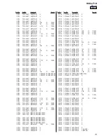


60
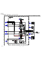
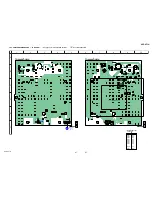
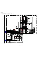
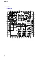
HCD-LF1H
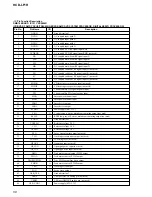
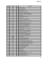
Pin No.
Pin Name
I/O
Description
231
JITFN
I
Negative input of operation amplifier for RF jitter meter (not used)
232
PLLVSS
—
Ground terminal
233
IDAC
—
Not used
234
PLLVDD3
—
Power supply (RF+3.3V)
235
LPFON
O
Negative output of loop filter amplifier
236
LPFIP
I
Positive input of loop filter amplifier
237
LPFIN
I
Negative input of loop filter amplifier
238
LPFOP
O
Positive output of loop filter amplifier
239
VDD3
—
Power supply (RF+3.3V)
240
VCM
I
Not used
241
VSS
—
Ground terminal
242
VREFP
I
SACD top reference
243
VREFN
I
SACD bottom reference
244
RFVDD3
—
Power supply (RF+3.3V)
245
RFRPDC
I
RFRP signal input
246
RFRPAC
I
RFRP signal input
247
HRFZC
I
High frequency RF ripple zero crossing
248
CRTPLP
O
Defect level filter capacitor connecting
249
RFGND
—
Ground terminal
250
CEQP
—
Not used
251
CEQN
—
Not used
252
OSP
I
RF offset cancellation capacitor connecting
253
OSN
O
RF offset cancellation capacitor connecting
254
RFGC
O
RF offset loop capacitor connecting for DVD-ROM
255
IREF
I
Current reference input (Pull down)
256
AVDD3
—
Power supply (RF+3.3V)
Summary of Contents for HCD-LF1H
Page 78: ...78 HCD LF1H MEMO ...