86
HCD-HDX500/HDX501W
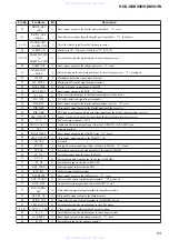
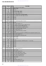
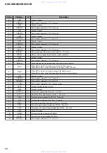
Pin No.
Pin Name
I/O
Description
49
USB_VDD3
-
Power supply terminal (+3.3V)
50
SPFG
I
Spindle motor hall sensor input from the motor driver
51
MSW
O
CD/DVD selection signal output terminal "L": CD, "H": DVD
52
CKSW
I
Chucking detection switch input terminal Not used
53
OCSW
I
Disc table open/close detection switch input terminal Not used
54
EEWP
O
Write protect signal output to the EEPROM
55
DVDD18
-
Power supply terminal (+1.8V)
56 to 64
HA2 to HA8,
HA18, HA19
O
Address signal output to the flash ROM
65
DVDD3
-
Power supply terminal (+3.3V)
66
XWR
O
Write enable signal output to the flash ROM
67 to 75
HA16 to HA9,
HA20
O
Address signal output to the flash ROM
76
XROMCS
O
Chip select signal output to the flash ROM
77
HA1
O
Address signal output to the flash ROM
78
XRD
O
Read enable signal output to the flash ROM
79, 80
HD0, HD1
I/O
Two-way data bus terminal with the flash ROM
81
DVSS
-
Ground terminal
82 to 86
HD2 to HD6
I/O
Two-way data bus terminal with the flash ROM
87
HA21
O
Address signal output to the flash ROM
88
RESERVED
-
Not used
89
HD7
I/O
Two-way data bus terminal with the flash ROM
90
DVSS
-
Ground terminal
91, 92
HA17, HA0
O
Address signal output to the flash ROM
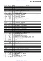
93
DVDD18
-
Power supply terminal (+1.8V)
94, 95
RESERVED
-
Not used
96
DVDD3
-
Power supply terminal (+3.3V)
97
IFSDO
O
Serial data output to the system controller
98
IFCK
O
Serial data transfer clock signal output to the system controller
99
xIFCS
O
Chip select signal output to the system controller
100
IFSDI
I
Serial data input from the system controller
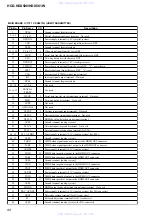
Serial data transfer clock signal output to the EEPROM and HDMI transmitter
Two-way data bus with the EEPROM and HDMI transmitter
Serial data transfer clock signal output to the HDMI OUT connector
Two-way data bus with the HDMI OUT connector
Receive data input terminal for UART communication when data writing to flash memory
Transmit data output terminal for UART communication when data writing to flash memory
ICE mode enable signal input terminal Not used
Reset signal input from the system controller "L": reset
110
xTXINT
O
Interrupt request signal output terminal Not used
111
DQM0
O
Data mask signal output to the SD-RAM
112
IFBSY
I
Busy signal input from the system controller
113 to 117
RD7 to RD3
I/O
Two-way data bus with the SD-RAM
118
DVDD3
-
Power supply terminal (+3.3V)
119 to 129
RD2 to RD0,
RD15 to RD8
I/O
Two-way data bus with the SD-RAM
130
LIMITSW
I
Limit detection switch input terminal
www. xiaoyu163. com
QQ 376315150
9
9
2
8
9
4
2
9
8
TEL 13942296513
9
9
2
8
9
4
2
9
8
0
5
1
5
1
3
6
7
3
Q
Q
TEL 13942296513 QQ 376315150 892498299
TEL 13942296513 QQ 376315150 892498299


