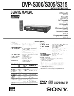
background image

MICROFILM

SERVICE MANUAL

US Model

DVP-S300

E Model

DVP-S300/S305

AEP Model

DVP-S315

UK Model

DVP-S315

Chinese Model

DVP-S305

Taiwan Model

DVP-S305

Singapore Model

DVP-S305

CD/DVD PLAYER

DVP-S300/S305/S315

RMT-D103E/105A/105P

SPECIFICATIONS

CD/DVD player

Signal format system

PAL/ (NTSC): DVP-A305/S315
NTSC

: DVP-S300

Audio characteristics

Frequncy response

DVD (PCM 96 kHz): 2 Hz to 44 kHz
(+0.5 dB, –2.0 dB)
DVD (PCM 48 kHz): 2 Hz to 22 kHz
(±0.5 dB)
CD: 2 Hz to 20 kHz (±0.5 dB)

Signal-to-noise ratio

More than 107 dB (LINE OUT (AUDIO)
connectors only)

Harmonic distortion

Less than 0.0028%

Dynamic range

More than 100 dB (DVD)
More than 97 dB (CD)

Wow and flutter

Less than detected value
(±0.001% W PEAK)

Outputs and inputs

jack

Output

Load impedance

type

level

LINE OUT

Phono

2 Vrms

Over 10 kilohms

(AUDIO)

jacks

(at 50 kilohms)

DIGITAL OUT

Optical

–18 dBm

Wave length: 660 nm

(OPTICAL)

output
connector

DIGITAL OUT

Phono

0.5 Vp-p

75 ohms terminated

(COAXIAL)

jacks

LINE OUT

Phono

1.0 Vp-p

75 ohms,

(VIDEO)

jack

sync negative

S VIDEO OUT

4-pin mini

Y: 1.0 Vp-p 75 ohms,

DIN

sync negative

C: 0.3 Vp-p 75 ohms terminated

PHONES

Phone

12 mW

32 ohms

jack

General

Power requirements

220 – 240 V AC, 50 Hz: DVP-S305/S315
120 V AC, 60 Hz: DVP-S300

Power consumption

22 W: DVP-S305/S315
20 W: DVP-S300

Dimensions (approx.)

430 

×

 95 

×

 325 mm (17 

×

 3

3

/

4


×

 12

7

/

8

 in.)

(w/h/d): DVP-S300/S315
430 

×

 95 

×

 330 mm (w/h/d): DVP-S305

incl. projecting parts

Mass (approx.)

4.0 kg (8 lb 13 oz)

Operating temperature

41 

°

F to 95 

°

F (5 

°

C to 35

°

C)

Operating humidity

5% to 90%

Supplied accessories

• Audio/video/S-link connecting cord (1) (DVP-S300: US)
• Audio/Video connecting cord (1)

(DVP-S300: E/S305/S315)

• S video cable (1)
• Remote commander (remote) RMT-D103E (1) (DVP-S305)
• Remote commander (remote) RMT-D105A (DVP-S300)
• Remote commander (remote) RMT-D105P (DVP-S315)
• sony R6 (size AA) batteries (2)

Design and specifications are subject to change without notice.

Summary of Contents for DVP-S300

Page 1: ...cal 18 dBm Wave length 660 nm OPTICAL output connector DIGITAL OUT Phono 0 5 Vp p 75 ohms terminated COAXIAL jacks LINE OUT Phono 1 0 Vp p 75 ohms VIDEO jack sync negative S VIDEO OUT 4 pin mini Y 1 0 Vp p 75 ohms DIN sync negative C 0 3 Vp p 75 ohms terminated PHONES Phone 12 mW 32 ohms jack General Power requirements 220 240 V AC 50 Hz DVP S305 S315 120 V AC 60 Hz DVP S300 Power consumption 22 W...

Page 2: ...out to the customer and recom mend their replacement 5 Check the line cord for cracks and abrasion Recommend the replacement of any such line cord to the customer 6 Check the B voltage to see it is at the values specified 7 Check the antenna terminals metal trim metallized knobs screws and all other exposed metal parts for AC leakage Check leakage as described below SAFETY CHECK OUT After correcti...

Page 3: ...Boards 4 61 FL 88 FR 133 Schematic Diagrams 4 65 ER 2 Schematic Diagram 4 69 ER 2 Printed Wiring Board 4 73 Power Block HS 930SF Printed Wiring Board and Schematic Diagram 4 78 Power Block HS 930SH Printed Wiring Board and Schematic Diagram 4 81 Power Block HS 930SU Printed Wiring Board and Schematic Diagram 4 84 5 IC PIN FUNCTION DESCRIPTION 5 1 Interface Control Pin Function MB 78 Board IC604 5 ...

Page 4: ... Board Page 2 1 Front Panel Section Page 2 1 AU 197 Board Page 2 1 MD Block Ass y Page 2 2 Optical Pick up Page 2 3 Skew Motor Page 2 2 Spindle Base Page 2 3 Sled Motor Page 2 3 Spindle Motor Page 2 3 Set 1 DISASSEMBLY This set can be disassembled in the order shown below ...

Page 5: ...ear 1 in direction A See Fig 2 Note To prevent a damege of cam gear rotate it in direction A by 1 4 turn 2 Draw out the tray 2 in direction B by hand and remove a disk See Fig 2 Fig 2 4 HOW TO SERVICE MB 78 BOARD 1 Remove the case from the set Refer to 2 1 2 Remove the cover upper Refer to 2 3 3 Set the MB 78 board as shown in Fig 3 Note Do not disconnect wiring Fig 3 Two tapping screws Two tappin...

Page 6: ...e MD block ass y 3 90 º with the side down confirm that the optical pick up 4 falls by self weight See Fig 5 4 Further with the front side of MD block ass y 3 up confirm that the optical pick up falls by self weight Fig 5 1 Sled motor ass y 2 Two screws M1 7 2 5 A 3 MD block ass y 4 Optical pick up Upper Lower Front side Upper Lower Front side ...

Page 7: ...parts the short lands have been soldered to protect from static electricity Accordingly remove solders when replacing opti cal pick up See Fig 6 Fig 6 Flexible board 3 In handling the KHS 180A RP do not touch inhibited parts shown in Fig 7 but grip the slide base bearing and U shaped guide Fig 7 KHS 180A RP Touch inhibited parts Objective lens Skew sensor Laser holder Laser coupler Flexible board ...

Page 8: ...nded grease is Foil KG 70MP Note 2 In applying grease take care not to allow grease to stick to other parts particularly rubber belt spindle motor and optical pick up Fig 8 Base unit holder 2 bosses Slide base Skew cam Cam gear Tray 3 grooves Note Add grease if tray moves slowly Loading pulley shaft Note Add grease if tray generates noise periodically ...

Page 9: ...unction normally if the board floats up Fig 12 7 2 Cleaning Spindle Motor Turntable 1 Remove the tray Refer to 2 7 2 Clean the spindle motor turntable if disc antiskid rubber black is dirty See Fig 9 Fig 9 7 3 Aligning Phase of Cam Gear and Drive Gear 1 Align triangle marks when assembling the cam gear and drive gear See Fig 10 Fig 10 Spindle motor Turntable Four step screws Two insulators Two ins...

Page 10: ...screws BV3 10 The sensor will not function normally if the board floats up Fig 13 7 7 Note on connecting OPT Harness 1 The optical pick up could be destroyed unless the OPT har ness is connected normally to the connector See Fig 14 Fig 14 TK 47 board Three screws BV3 10 Two claws Boss Two claws Boss OPT harness Connector Good NG ...

Page 11: ...1 1 SECTION 1 GENERAL DVP S300 S305 S315 This section is extracted from DVP S315 instruction manual ...

Page 12: ...1 2 ...

Page 13: ...1 3 ...

Page 14: ...1 4 ...

Page 15: ...1 5 ...

Page 16: ...1 6 ...

Page 17: ...1 7 ...

Page 18: ...1 8 ...

Page 19: ...1 9 ...

Page 20: ...1 10 1 10 E ...

Page 21: ...ion 3 Rotate the cam gear in direction A Claw 9 Lug 8 Screw B3 2 Flat cable 4 Draw out the tray by hand Two claws 6 Tray ornamental panel ass y 5 Two claws 0 Claw 7 Screw B3 Cam gear 0 Four flat cables CN101 252 301 452 1 Two connectors CN001 002 4 Connector CN361 5 Two screws B3 3 Flat cable CN251 S315 8 Two screws B3 2 Two flat cables CN301 601 6 Three screws B3 7 Cover upper 9 MB 78 board 6 Two...

Page 22: ...s B3 3 Chassis bracket B 1 Cover lower 6 Clamp 2 Flat cable spindle motor CN002 1 Connector CN004 5 Two claws 3 OP 15 flexible board CN001 4 Four screws BVTP3 10 6 TK 47 board A 3 Rotate the cam gear in direction A 5 Claw 6 Remove the tray 4 Pull the tray 2 Press pully bracket 1 Two screws BVTP3 10 2 Claw 4 Skew motor M902 3 Skew gear retainer 1 Screw PTTWH2 5 ...

Page 23: ...MOTOR M901 REMOVAL 1 OP 15 flexible board CN001 3 Skew shaft stopper 2 Screw P2 8 7 Sled motor M501 5 Screw PTTWH2 5 6 Two screws P1 7 2 5 4 Spindle base 1 Three screws PTTWH2 5 2 Spindle motor M901 1 OP 15 flexible board CN001 2 Screw PTTWH2 5 3 Main shaft 4 Optical pick up ...

Page 24: ...HS 180A J1N 8 820 005 02 Skew motor ass y X 3947 138 1 Sled motor ass y X 3947 137 1 DC motor spindle 1 698 944 11 Sled motor ass y X 3947 137 1 Optical pick up KHS 180A J1N 8 820 005 02 Motor loading 1 698 942 21 DC motor spindle 1 698 944 11 ...

Page 25: ...S315 HEAD PHONE ME 15 S305 MIC IN FR 133 IR POWER SWITCH DC MOTOR SPINDLE FL 88 FL DRIVER FUNCTION SWITCH TK 47 RF SERVO ER 2 S315 EURO AV AU 197 AUDIO FG 43 SLED POWER BLOCK HS 930SF S300 E S305 Taiwan E HS 930SH S315 S305 Chinese Singapore HS 930SU S300 US SWITCHING REGULATOR ...

Page 26: ... Address and data set 93 100 A8 15 I O Set address 5 1 INTERFACE CONTROL PIN FUNCTION IC604 on MB 78 Board 6 8 Pin No Pin Name I O Function Pin No Pin Name I O Function 1 4 A16 19 I O Set Address 5 6 TIN0 1 Not used 7 8 TOT0 1 Not used 9 ALE O Output of address latch inable signal 10 OE O Output of output inable signal 11 GND GND 12 WRL O Output of write inable signal 13 WRH Not used 14 HRQ Not us...

Page 27: ...0 O Output of A mute signal 65 PA11 O Output of MA mute signal 66 IRQ0 I Input of interrupt fromIC203 67 IRQ1 I Input of DMA request from IC203 68 IRQ2 I Input of V SYNC FID interrupt signal 69 IRQ3 I Input of interrupt from IC804 70 VCC Digital power supply 71 CK O Output of internal clock 72 VSS Digital ground 73 EXTAL 20MHz crystal connection pin 74 XTAL 20MHz crystal connection pin 75 VCC Vpp ...

Page 28: ...t used 105 PB7 Not used 106 VSS Digital ground 107 RxD0 I Input of serial data 108 TxD0 O Output of serial data 109 RxD1 I Input of serial data 110 TxD1 O Output of serial data 111 SCK0 O Output of serial clock 112 SCK1 O Output of serial clock Pin No Pin Name I O Function ...

Page 29: ... 2 ROM Check As item No is 2 2 enter 0202 Syscon Diagnosis IF con Ver 0 620 9315 SYScon Ver 0 400 0000 Select Diag No 0 Enter item No 0 Press Remocon Key SIRCS FF KEY FF Figure 3 Syscon Diagnosis IF con Ver 0 620 9315 SYScon Ver 0 400 0000 Select Sub No 02 Enter item No 02 Press Remocon Key SIRCS FF KEY FF Figure 4 Syscon Diagnosis IF con Ver 0 620 9315 SYScon Ver 0 400 0000 Select Sub No 02 0 Ent...

Page 30: ...external RAM IC802 are checked twice by inverting the data but in the simple check one block is checked then the subsequent 4 blocks are skipped and also a check of in verted data is not executed If write read mismatch error occurred checking can be repeated 3 Destination Setting 3 2 Destination setting Check I O port read Error Not detected The destination setting port I O is read and displayed w...

Page 31: ... is initialized by the reset is checked First the version No is read then its comple ment is written After hardware reset the data is read again and if it matches the written data the reset error occurs 6 Data Source 6 2 Register in ARP IC806 Register write Register read matching check Error 05 Write read data mismatch error Data from 0x00 up to 0xff are written to 12 registers where all bits can ...

Page 32: ...ters where all bits can be written read then they are read to check for matching If write read mismatch error occurred checking can be repeated 7 3 Reset Line in 64020 Register write Hard reset Register read matching check Error 02 Reset error 05 Write read data mismatch error After 0xff is written to the Capture Compare Control Register 0 whether it is initialized to 0x00 by the reset pulse signa...

Page 33: ... be 12 times exactly but 1 errors are allowable 8 5 Still Picture Output SDRAM IC201 202 direct write Pattern data AV Decoder IC203 Video Out Error 31 AV Decoder IC203 interruption DMA transfer is not detected The pattern is directly written to the SDRAM IC201 202 in AV Decoder IC203 then its picture display is checked First the brightness signal data are written by the amount of one screen while ...

Page 34: ... S315 Color bar output by video encoder Error 11 Serial transfer error With AV CONT H VS H video signals are output For the video signals the color bars are output same as in 8 2 8 13 AV CONT Through Check DVP S315 Color bar output by video encoder Error 11 Serial transfer error Input picture is sent as it is from EURO AV2 CNJ601 to the AV1 CNJ602 The color bars are output from the player same as ...

Page 35: ...ia ARP IC806 and analog audio data are output from 2ch DAC IC215 If no error is found the message is displayed to prompt for key entry 9 8 Dual DAC Serial ROM audio data ARP IC806 AV Decoder IC203 2ch DAC IC215 Analog audio output Attenuation Error 10 ARP IC806 AV Decoder IC203 data transfer error 35 2ch DAC IC215 serial transfer interruption is not de tected 37 PLL DAC IC209 serial transfer inter...

Page 36: ...ed 37 PLL DAC interruption is not detected 40 1914 ID error 41 Vsync interruption is not detected 42 Vsync interrupt cycle error 43 AC 3 DAC for main interruption is not detected 44 AC 3 DAC for center interruption is not detected 45 AC 3 DAC for surrounding interruption is not detected 52 DIR interruption is not detected 53 V ENC CXD1914 interruption is not detected 54 Karaoke DSP CXD2721Q interr...

Page 37: ...ng ON Sled ON AGC ON CLVA Lock Check Auto Loop Filter Offset Auto Focus Offset Auto Tilt Offset Auto Focus Offset servo stop Go To Home Position LD ON Spindle start Tilt ON Focus ON FOK Check Tan Position FOK Check Tracking ON Sled ON AGC ON CLVA Lock Check Tangential skew adjustment 10k tj rev 3 STOP STOP STOP STOP 4 NG OK NG OK NG OK NG OK NG OK NG OK NG OK NO YES NO YES Drive Automatic Adjustme...

Page 38: ...e Position Disc Type Check NG OK LD ON Spindle start Tilt ON Focus ON 5 STOP 4 2 6 Tracking ON Sled ON CLVA Auto Tracking Offset FOK Check STOP NG OK Lock Check STOP NG OK Auto Loop Filter Offset Auto Focus Offset Auto Focus Gain Auto Tracking Gain Auto Loop Filter Offset Pull in Memory Jitter Check Servo STOP Search Check STOP NG OK OK Select ALL or DVD_DL NO YES Eject Disc change CD n DVD_DL Loa...

Page 39: ... ON Sled ON AGC ON CLVA Lock Check STOP NG OK NG OK Auto Focus Offset Auto Tilt Offset Auto Focus Offset Auto Focus Gain Auto Tracking Gain Auto EQ Layer Check Jitter Check STOP STOP NG OK OK NG Focus Jump L0 n L1 10 FOK Check Tracking ON Sled ON CLVA Layer Check STOP STOP NG OK NG OK DVD_DL adjustment Lock Check Auto Focus Offset Auto Tilt Offset Auto Focus Offset Auto Focus Gain Auto Tracking Ga...

Page 40: ...re 9 is displayed Drive Auto Adjustment SA 00000 SI 00 EMG OO 0 Adjustment ALL 0 All 2 CD 2 DVD SL 3 DVD DL START Press ENTER Key Blinking STOP Press STOP Key Figure 9 The tray opens after the ENTER key is pressed and the initializa tion is finished Then place the DVD_SL disc for adjustment Press the ENTER key to start adjustment During adjustment the tan gential skew adjustment screen is displaye...

Page 41: ...forming manual operation observe the following points Select correct disc type on the Disc Type screen First select 0 Disc TYpe and execute 7 Hydet init and 8 Sled init See Figure 11 In case of abnormality press stop immediately to stop operation and turn off the power Do not execute Auto Adjust while executing FG Pause Also as these commands are not protected take care not to press wrong key When...

Page 42: ...Jump 10k tracks reversely direct search 6 FJ0 1 After layer jump L0 L1 tracking loop does not turn on 7 FJ1 0 After layer jump L1 L0 tracking loop does not turn on 8 LJ0 1 After layer jump L0 L1 tracking loop turns on 9 LJ1 0 After layer jump L1 L0 tracking loop turns on FWD 1TJ Jump one track forward RVS 1TJ Jump one track reversely 6 6 6 Manual Adjust 1 Manual Adjust 1 SA 000000 SI CD EMG 00 0 T...

Page 43: ...s after focus offset and tangential skew are adjusted 2 Auto Focus Offset Adjust focus offset automatically Adjusted result is reflected on the EEPROM Execute this with CLVA turned on If NG retry this after tilt offset and tangential skew are ad justed 30 3 Auto Focus Gain Adjust focus gain automatically Adjusted result is reflected on the EEPROM Execute this with CLVA turned on if possible If NG ...

Page 44: ... Gain 00 7F 20 center DVD_SL Tilt Offset 00 FF 80 center DVD_SL Pullin Level 80 FF D0 center DVD_SL EQ Boost Fixed according to the disc type L F O Only lower 5 bits are effective SD About 50 E0 HY About 60 A0 6 7 Other Operation For manual operation of the drive the following operations are available besides the operations given on the menu screen Com mon to front panel and remote commander Eject...

Page 45: ... Confirm that each voltage satisfies the specification SECTION 7 ELECTRICAL ADJUSTMENT DVP S300 S305 S315 In making adjustment refer to 7 4 Adjustment Related Parts Arrangement Note During diagnostic check the characters and color bars can be seen only with the NTSC monitor Therefore for diag nostic check use the monitor that supports both NTSC and PAL modes This section describes procedures and i...

Page 46: ...Diagnosis set so that CXD1914 color bars are generated 2 Adjust the RV251 to attain 1 0 02 Vp p Figure 7 2 2 S terminal Output Check MB 78 board Purpose Check S terminal video output If it is incorrect pictures will not be displayed correctly in spite of connection to the TV with an S terminal cable Mode CXD1914 ENC check in test mode menu 0 Syscon Diagnosis Signal Color bars Test point CN252 0 pi...

Page 47: ...to select S terminal 5V Confirm that the voltage at CN252 pin is 5 0 V 0 1 5 0 1 5 1 0 05 Vp p 286 20 mVp p 11 12 100µF 75Ω 1 100k 1 CN252 Digital voltmeter 11 12 100µF 75Ω 1 100k 1 CN252 Oscilloscope 700 30 mVp p 4 Checking Component Video Output R Y MB 78 board DVP S315 only Purpose This checks component video output R Y If it is incorrect cor rect colors will not be displayed when connected to ...

Page 48: ...7 4 7 4 Adjustment Related Parts Arrangement MB 78 BOARD Side A 1 9 CN251 CT201 27MHz FREERUN 1 7 8 14 IC206 RV251 VIDEO LEVEL CN201 1 4 6 8 9 11 12 14 HS 930SF 930SH 930SU BOARD Side A ...

Page 49: ...7 5 E 1 2 10 12 14 24 25 CN252 MB 78 BOARD Side B ...

Page 50: ...r dotted line with mark are criti cal for safety Replace only with part number speci fied Ref No Part No Description Remark Ref No Part No Description Remark 8 1 1 CASE ASSEMBLY 4 3 988 027 01 CASE S300 S315 4 3 988 027 11 CASE S305 E Singapore 4 3 988 027 21 CASE S305 Taiwan Chinese 5 1 475 686 51 COMMANDER STANDARD RMT D103E S305 5 1 475 688 11 COMMANDER STANDARD RMT D105A S300 5 1 475 688 21 CO...

Page 51: ... 4 963 404 81 EMBLEM 5 A SONY S305 Taiwan Chinese 58 3 988 031 01 BUTTON OPEN S300 S315 58 3 988 031 11 BUTTON OPEN S305 E Singapore 58 3 988 031 21 BUTTON OPEN S305 Taiwan Chinese 59 4 951 620 01 SCREW 2 6X8 BVTP 60 3 945 284 51 KNOB VOLUME S300 S315 60 3 945 284 61 KNOB VOLUME S305 E Singapore 60 3 945 284 71 KNOB VOLUME S305 Taiwan Chinese 61 3 950 989 01 NUT M7 HEXAGON 62 3 684 436 01 PLATE MO...

Page 52: ...11 CABLE FLAT FMA 4 25P 108 1 783 353 11 CABLE FLAT FEA 2 15P S315 109 A 6065 108 A ER 2 BOARD COMPLETE S315 110 1 777 850 51 CORD POWER US 110 1 777 851 41 CORD POWER E Singapore 110 1 782 001 61 CORD POWER AEP UK 110 1 782 692 31 CORD POWER Chinese 110 1 777 985 51 CORD POWER Taiwan 111 3 490 052 01 LABEL LASER CLASS 1 S315 112 3 703 150 11 CLAMP 113 1 500 386 11 FILTER CLAMP FERRITE CORE S315 T...

Page 53: ...071 01 PULLEY LOADING 157 3 669 596 00 WASHER 2 3 STOPPER 158 3 975 070 01 BELT 159 3 975 085 01 PULLEY MOTOR 160 3 975 089 01 BRACKET PRESS PULLEY 161 3 975 074 01 PULLEY PRESS 162 3 975 077 01 SCREW BU STOPPER 163 3 975 088 01 HOLDER BASE UNIT 164 X 3948 398 1 HOLDER ASSY MD 165 A 6065 077 A TK 47 BOARD COMPLETE 166 4 981 923 01 SCREW M STEP M902 1 698 942 21 MOTOR LOADING not supplied M902 3 7 ...

Page 54: ...65 078 A FG 43 BOARD COMPLETE 212 1 783 341 11 CABLE FLAT FMF 28 8P 213 3 975 059 01 RETAINER SKEW GEAR 214 3 975 057 01 GEAR SKEW 215 4 974 711 01 SCREW 2X5 P TYIGHT PTTWH 216 4 974 725 01 SCREW M1 7X2 5 P 218 A 4683 008 A GEAR ASSY LIMITTER 219 4 974 720 01 GEAR S B 220 4 974 726 01 GEAR S A M501 X 3947 137 1 MOTOR ASSY SLED M901 1 698 944 11 MOTOR DC SPINDLE M903 X 3947 138 1 MOTOR ASSY SKEW Th...

Page 55: ... 11 FILM 0 1uF 5 63V C233 1 164 232 11 CERAMIC CHIP 0 01uF 50V C234 1 130 467 00 MYLAR 470PF 5 50V C235 1 126 926 11 ELECT 1000uF 20 10V C236 1 130 467 00 MYLAR 470PF 5 50V C239 1 126 967 11 ELECT 47uF 20 16V S300 S305 C239 1 124 910 11 ELECT 47uF 20 50V S315 C240 1 126 967 11 ELECT 47uF 20 16V S300 S305 C240 1 124 910 11 ELECT 47uF 20 50V S315 C245 1 126 964 11 ELECT 10uF 20 50V C264 1 164 232 11...

Page 56: ...ACK PIN 1P DIGITAL OUT COAXIAL J354 1 694 409 41 TERMINAL BOARD LINE OUT S300 S305 J354 1 694 408 41 TERMINAL BOARD LINE OUT S315 COIL L351 1 414 930 21 INDUCTOR 2 2uH L352 1 414 930 21 INDUCTOR 2 2uH L354 1 414 926 21 INDUCTOR 0 47uH L355 1 412 951 11 INDUCTOR 10uH L356 1 412 951 11 INDUCTOR 10uH L357 1 412 951 11 INDUCTOR 10uH TRANSISTOR Q201 8 729 424 08 TRANSISTOR UN2111 S300 S315 Q202 8 729 2...

Page 57: ... R383 1 216 017 91 RES CHIP 47 5 1 10W R384 1 216 295 91 SHORT 0 R385 1 216 295 91 SHORT 0 R386 1 216 295 91 SHORT 0 S315 A 6065 108 A ER 2 BOARD COMPLETE S315 Ref No 2 000 Series CAPACITOR C601 1 164 232 11 CERAMIC CHIP 0 01uF 50V C602 1 128 551 11 ELECT 22uF 20 25V C603 1 126 967 11 ELECT 47uF 20 16V C604 1 126 967 11 ELECT 47uF 20 16V C605 1 164 232 11 CERAMIC CHIP 0 01uF 50V C606 1 164 232 11 ...

Page 58: ...SISTOR UN2213 Q638 8 729 421 19 TRANSISTOR UN2213 Q639 8 729 422 27 TRANSISTOR 2SD601A Q Q640 8 729 421 19 TRANSISTOR UN2213 Q641 8 729 421 19 TRANSISTOR UN2213 C675 1 163 251 11 CERAMIC CHIP 100PF 5 50V C676 1 163 251 11 CERAMIC CHIP 100PF 5 50V C686 1 163 251 11 CERAMIC CHIP 100PF 5 50V C687 1 163 251 11 CERAMIC CHIP 100PF 5 50V C694 1 163 009 11 CERAMIC CHIP 0 001uF 10 50V C695 1 163 009 11 CER...

Page 59: ...00 METAL CHIP 15K 5 1 10W R667 1 216 049 91 RES CHIP 1K 5 1 10W R668 1 216 049 91 RES CHIP 1K 5 1 10W R669 1 216 073 00 METAL CHIP 10K 5 1 10W R670 1 216 073 00 METAL CHIP 10K 5 1 10W R671 1 216 073 00 METAL CHIP 10K 5 1 10W R672 1 216 073 00 METAL CHIP 10K 5 1 10W R673 1 216 073 00 METAL CHIP 10K 5 1 10W R674 1 216 073 00 METAL CHIP 10K 5 1 10W R675 1 216 049 91 RES CHIP 1K 5 1 10W R676 1 216 049...

Page 60: ...P 1K 5 1 10W R119 1 216 091 00 METAL CHIP 56K 5 1 10W R120 1 216 073 00 METAL CHIP 10K 5 1 10W R123 1 216 073 00 METAL CHIP 10K 5 1 10W R124 1 216 063 91 RES CHIP 3 9K 5 1 10W R126 1 216 009 00 METAL CHIP 22 5 1 10W R127 1 216 063 91 RES CHIP 3 9K 5 1 10W R128 1 216 077 00 METAL CHIP 15K 5 1 10W R129 1 216 061 00 METAL CHIP 3 3K 5 1 10W R130 1 216 025 91 RES CHIP 100 5 1 10W R131 1 216 025 91 RES ...

Page 61: ...RES CHIP 47K 5 1 10W R004 1 216 089 91 RES CHIP 47K 5 1 10W R005 1 216 081 00 METAL CHIP 22K 5 1 10W R006 1 216 081 00 METAL CHIP 22K 5 1 10W R007 1 216 049 91 RES CHIP 1K 5 1 10W R008 1 216 049 91 RES CHIP 1K 5 1 10W R009 1 216 049 91 RES CHIP 1K 5 1 10W R010 1 216 049 91 RES CHIP 1K 5 1 10W R011 1 216 295 91 SHORT 0 R012 1 216 295 91 SHORT 0 VARIABLE RESISTOR RV001 1 225 606 11 RES VAR CARBON 10...

Page 62: ... CHIP 15PF 5 50V S315 C271 1 162 921 11 CERAMIC CHIP 33PF 5 50V S300 S305 C272 1 162 917 11 CERAMIC CHIP 15PF 5 50V C281 1 107 826 11 CERAMIC CHIP 0 1uF 10 16V S315 C282 1 107 826 11 CERAMIC CHIP 0 1uF 10 16V S315 C301 1 162 967 11 CERAMIC CHIP 0 0033uF 10 50V C303 1 126 193 11 ELECT 1uF 20 50V C304 1 162 967 11 CERAMIC CHIP 0 0033uF 10 50V C305 1 165 176 11 CERAMIC CHIP 0 047uF 10 16V C306 1 162 ...

Page 63: ...V C539 1 107 826 11 CERAMIC CHIP 0 1uF 10 16V C540 1 162 970 11 CERAMIC CHIP 0 01uF 10 25V C541 1 128 004 11 ELECT CHIP 10uF 20 16V C542 1 107 826 11 CERAMIC CHIP 0 1uF 10 16V C543 1 128 004 11 ELECT CHIP 10uF 20 16V C544 1 162 970 11 CERAMIC CHIP 0 01uF 10 25V C545 1 162 970 11 CERAMIC CHIP 0 01uF 10 25V C546 1 162 970 11 CERAMIC CHIP 0 01uF 10 25V C547 1 162 970 11 CERAMIC CHIP 0 01uF 10 25V C54...

Page 64: ...70 11 CERAMIC CHIP 0 01uF 10 25V C863 1 162 970 11 CERAMIC CHIP 0 01uF 10 25V C864 1 126 206 11 ELECT CHIP 100uF 20 6 3V C865 1 162 970 11 CERAMIC CHIP 0 01uF 10 25V CONNECTOR CN001 1 778 768 21 PIN CONNECTOR PC BOARD 8P CN002 1 784 687 41 PIN CONNECTOR PC BOARD 7P CN101 1 774 769 11 CONNECTOR FFC FPC 25P CN251 1 770 692 11 CONNECTOR FFC FPC 9P S315 CN252 1 774 769 11 CONNECTOR FFC FPC 25P CN301 1...

Page 65: ... 701 39 IC NJM3404AM IC302 8 759 384 55 IC LA6527N TE B IC303 8 759 333 63 IC LB1896 TE B IC361 8 759 490 71 IC BA5912AFP YE2 IC363 8 759 522 13 IC BA5981FP E2 IC452 8 759 441 31 IC MC14053BDTR2 IC455 8 759 100 93 IC uPC393G2 IC501 8 759 100 93 IC uPC393G2 IC502 8 759 701 36 IC NJM3403AM TE2 IC503 8 759 701 36 IC NJM3403AM TE2 IC506 8 759 525 61 IC CXD8730R IC507 8 759 701 39 IC NJM3404AM IC508 8 ...

Page 66: ...AL CHIP 47 5 1 16W R195 1 216 805 11 METAL CHIP 47 5 1 16W R196 1 216 805 11 METAL CHIP 47 5 1 16W R197 1 216 805 11 METAL CHIP 47 5 1 16W R198 1 216 805 11 METAL CHIP 47 5 1 16W R199 1 216 805 11 METAL CHIP 47 5 1 16W R200 1 216 801 11 METAL CHIP 22 5 1 16W R202 1 216 805 11 METAL CHIP 47 5 1 16W R203 1 216 805 11 METAL CHIP 47 5 1 16W R204 1 216 805 11 METAL CHIP 47 5 1 16W R205 1 216 864 11 MET...

Page 67: ...216 833 11 METAL CHIP 10K 5 1 16W R302 1 216 845 11 METAL CHIP 100K 5 1 16W R304 1 216 841 11 METAL CHIP 47K 5 1 16W R305 1 216 839 11 METAL CHIP 33K 5 1 16W R306 1 216 833 11 METAL CHIP 10K 5 1 16W R307 1 216 853 11 METAL CHIP 470K 5 1 16W R308 1 216 845 11 METAL CHIP 100K 5 1 16W R309 1 216 833 11 METAL CHIP 10K 5 1 16W R313 1 216 833 11 METAL CHIP 10K 5 1 16W R314 1 216 821 11 METAL CHIP 1K 5 1...

Page 68: ...09 11 METAL CHIP 100 5 1 16W R486 1 216 821 11 METAL CHIP 1K 5 1 16W R487 1 216 821 11 METAL CHIP 1K 5 1 16W R488 1 216 857 11 METAL CHIP 1M 5 1 16W R489 1 216 819 11 METAL CHIP 680 5 1 16W R490 1 216 839 11 METAL CHIP 33K 5 1 16W R491 1 216 833 11 METAL CHIP 10K 5 1 16W R492 1 216 839 11 METAL CHIP 33K 5 1 16W R493 1 216 833 11 METAL CHIP 10K 5 1 16W R494 1 216 819 11 METAL CHIP 680 5 1 16W R495 ...

Page 69: ... 11 METAL CHIP 1K 5 1 16W R631 1 216 821 11 METAL CHIP 1K 5 1 16W R632 1 216 833 11 METAL CHIP 10K 5 1 16W R633 1 216 809 11 METAL CHIP 100 5 1 16W R634 1 216 833 11 METAL CHIP 10K 5 1 16W R635 1 216 809 11 METAL CHIP 100 5 1 16W R636 1 216 821 11 METAL CHIP 1K 5 1 16W R637 1 216 833 11 METAL CHIP 10K 5 1 16W S300 US S305 E Taiwan Singapore R638 1 216 833 11 METAL CHIP 10K 5 1 16W R640 1 216 833 1...

Page 70: ...0 1 16W R852 1 218 871 11 RES CHIP 10K 0 50 1 16W R853 1 218 871 11 RES CHIP 10K 0 50 1 16W R854 1 216 809 11 METAL CHIP 100 5 1 16W R855 1 216 833 11 METAL CHIP 10K 5 1 16W R856 1 216 837 11 METAL CHIP 22K 5 1 16W R857 1 216 825 11 METAL CHIP 2 2K 5 1 16W R858 1 216 838 11 METAL CHIP 27K 5 1 16W R859 1 216 825 11 METAL CHIP 2 2K 5 1 16W R860 1 216 821 11 METAL CHIP 1K 5 1 16W R861 1 216 833 11 ME...

Page 71: ... INDUCTOR CHIP 0UH IC IC801 8 759 369 74 IC NJM4556AM TE2 IC802 8 759 453 78 IC BU9253FS E2 IC803 8 759 100 96 IC uPC4558G2 JACK J801 1 507 854 00 JACK PHONE MIC COIL L801 1 414 934 21 INDUCTOR 10uH TRANSISTOR Q802 8 729 023 22 TRANSISTOR 2SD2114KT146 Q803 8 729 421 19 TRANSISTOR UN2213 Q804 8 729 424 18 TRANSISTOR UN2113 RESISTOR R801 1 216 025 91 RES CHIP 100 5 1 10W R802 1 216 097 91 RES CHIP 1...

Page 72: ...5 01 TRANSISTOR 2SJ488 HS 930SH Q211 9 880 451 01 TRANSISTOR 2SJ488 HS 930SU Q311 8 729 921 42 TRANSISTOR 2SA1679 Q312 8 729 920 69 TRANSISTOR 2SC1740 Q511 8 880 440 01 TRANSISTOR 2SK2279 HS 930SU Q511 8 880 446 01 TRANSISTOR 2SK2279 HS 930SH Q511 8 880 452 01 TRANSISTOR 2SK2279 HS 930SF Q512 8 729 920 67 TRANSISTOR 2SA933S RESISITOR R152 1 219 121 21 FUSIBLE 0 22 1 4W A 6065 077 A TK 47 BOARD COM...

Page 73: ...9 420 24 TRANSISTOR 2SB1218A QRS Q004 8 729 805 25 TRANSISTOR 2SB1121 Q005 8 729 805 25 TRANSISTOR 2SB1121 Q007 8 729 805 25 TRANSISTOR 2SB1121 Q008 8 729 230 63 TRANSISTOR 2SC4116 YG Q009 8 729 015 76 TRANSISTOR UN5211 TX Q010 8 729 230 63 TRANSISTOR 2SC4116 YG RESISTOR R001 1 216 025 91 RES CHIP 100 5 1 10W R002 1 208 757 11 RES CHIP 91 0 50 1 10W R003 1 216 037 00 METAL CHIP 330 5 1 10W R005 1 ...

Page 74: ...2 TT B 3 7 685 647 79 SCREW BVTP 3X10 TYPE2 IT 3 7 7 627 852 08 SCREW PRECISION P 1 7X2 5 8 7 685 105 19 TPG P 2X8 TYPE 2 NON SLIT 9 7 627 852 17 P 1 7X4 ACCESSORIES PACKING MATERIALS 1 475 686 51 COMMANDER STANDARD RMT D103E S305 1 475 688 11 COMMANDER STANDARD RMT D105A S300 1 475 688 21 COMMANDER STANDARD RMT D105P S315 1 569 008 11 ADAPTOR CONVERSION 2P E 1 575 334 11 CORD CONNECTION STEREO AV...

Page 75: ... 176 Sony Corporation Home A V Products Company 9 921 680 11 DVP S300 S305 S315 98C0583 1 Printed in Japan 1998 3 Published by General Engineering Dept Osaki East ...

Reviews: