5-7
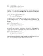
(5-6) Servo DSP reset line
Write into register
→
Resetting hardware
→
Read from register
Error
02: Reset error
13: Data Ready cannot be not set.
14: DSP download error
When testing the RAM version, confirm that the register can no more be read once the register is reset. When download error is not
detected, content of the DSP address 200h, is read. After resetting the hardware, the same content is read again so that the data are
compared. If any data cannot be read, or if the two data does not agree, result of this test is OK. When the data before hardware reset
and after the reset is the same, the reset error is output. In the ROM version, it is confirmed that value of version is initialized by
hardware reset. After reading the version value, its complement value is written. If the read-out value is the same as the written value,
the reset error is output.
(6) Data supply block
(6-2) ARP register
Write data into register
→
Read data from register and check if data agree
Error
05: Write data and read data do not agree.
Using the value of “0x00” to “0xff”, the 12 registers that can write and read data in all bits, are tested with “Data write-then-read
agreement check”. If write data and read data do not agree, check can be repeated.
(6-3) ARP reset line
Write into register
→
Resetting hardware
→
Read from register
Error
02: Reset error
05: Write data and read data do not agree.
The test is performed in the way that the data “0xfe” is written in the INTEN3 register, then the data is checked if the INTEN3 register
is initialized to “0x00” by the reset pulse signal. In addition to it, the read-data agreement check is performed for confirmation.
(6-4) ARP DRAM
ROM Data
→
ARP
→
DRAM
→
ARP reading, and check if data agrees.
Error
03: Data write error (ARP cannot be set into Write Enable.)
04: Data read error (ARP cannot be set into Read Enable.)
05: Write data and read data do not agree.
In this test, the ROM pattern is copied to the entire area to be checked. During this copying, address of the copy source (ROM) is
returned by 254 bytes after every copying of 256 bytes. When the detailed check mode is selected, the same check is repeated in order
to test all bits using the inverted data after the entire area has been checked.. The bus width of ARP is 16 bits. This check program shows
address in units of bit. By means of reading after writing data in the entire area, the overwriting by shadow can be checked.
In the detailed check mode, the entire area is checked twice using the inverted data. In the simple check mode, when one block is
checked, the succeeding four blocks are not checked. If write data and read data do not agree., check can be repeated.
(6-5) ARP interrupt line
Data transfer request
→
Interrupt from ARP that data transfer has ended.
Error
21: ARP interrupt is not detected.
The AC-3 audio data that is stored in ROM is transferred to ARP. The interrupt that data output from the specified sector of ARP has
ended, is detected. Because interrupt from Decrypt is supplied using the same interrupt line, the interrupts from Decrypt are all masked.
(6-6) Decrypt IC register
Write into register
→
Read from register and check if data agree
Error
05: Write data and read data do not agree.
The interrupt mask register is checked using the value of 0x00 to 0xfc (the lower two bits are masked) with the “Data write-then-read
agreement check” If write data and read data do not agree., check can be repeated.
Summary of Contents for DVP-M35
Page 9: ...1 1 DVP M35 SECTION 1 GENERAL This section is extracted from instruction manual ...
Page 10: ...1 2 ...
Page 11: ...1 3 ...
Page 12: ...1 4 ...
Page 13: ...1 5 ...
Page 14: ...1 6 ...
Page 15: ...1 7 ...
Page 16: ...1 8 ...
Page 17: ...1 9 ...
Page 18: ...1 10 ...
Page 19: ...1 11E ...
Page 32: ......
Page 34: ......
Page 43: ......
Page 45: ......
Page 46: ......
Page 48: ......
Page 50: ......


