background image

1-2

Summary of Contents for DVP-M35

Page 1: ...ong Kong Model Spanish Model E Model SERVICE MANUAL CD DVD PLAYER MICROFILM SPECIFICATIONS Refer to the OPERATION MANUAL 9 921 669 21 and DVD MECHANISM OPERATION MANUAL 9 921 669 31 for DVD mechanism DVP M35 RMT D102E ...

Page 2: ...ed 6 Flexible Circuit Board Repairing Keep the temperature of the soldering iron around 270 C during repairing Do not touch the soldering iron on the same conductor of the circuit board within 3 times Be careful not to apply force on the conductor when soldering or unsoldering SAFETY CHECK OUT After correcting the original service problem perform the following safety checks before releasing the se...

Page 3: ... 4 23 MB 78 INTERFACE SCHEMATIC DIAGRAM 4 26 MB 78 MOTOR DRIVE SCHEMATIC DIAGRAM 4 29 MB 78 POWER SUPPLY SCHEMATIC DIAGRAM 4 31 MB 78 DIGITAL PROCESS 1 SCHEMATIC DIAGRAM 4 33 MB 78 DIGITAL PROCESS 2 SCHEMATIC DIAGRAM 4 37 FG 43 SLED MOTOR HP 98 PHONES PRINTED WIRING BOARDS AND SCHEMATIC DIAGRAMS 4 41 AU 199 VIDEO AUDIO INPUT OUTPUT SCHEMATIC DIAGRAM 4 44 AU 199 VIDEO AUDIO INPUT OUTPUT PRINTED WIR...

Page 4: ... NOTE ON MOUNTING SLED MOTOR 1 Push the sled motor assy 1 toward direction A See Fig 2 2 Tighten two screws 2 M1 7 2 5 Fig 2 3 Raising the MD block assy 3 90 º with the side down confirm that the optical pick up 4 falls by self weight See Fig 3 4 Further with the front side of MD block assy 3 up confirm that the optical pick up falls by self weight DVP M35 1 Cam gear 2 Tray B A Screw Driver Fig 3 ...

Page 5: ... parts the short lands have been soldered to protect from static electricity Accordingly remove solders when replacing optical pick up See Fig 4 Fig 4 Flexible board 3 In handling the KHS 180A RP do not touch inhibited parts shown in Fig 5 but grip the slide base bearing and U shaped guide Touch inhibited parts Objective lens Skew sensor Laser holder Laser coupler Flexible board OEIC Lens actuator...

Page 6: ...nded grease is Foil KG 70MP Note 2 In applying grease take care not to allow grease to stick to other parts particularly rubber belt spindle motor and optical pick up Fig 6 Base unit holder 2 bosses Loading pulley shaft NOTE Add grease if tray generates noise periodically Tray 3 grooves NOTE Add grease if tray moves slowly Slide base Skew cam Cam gear ...

Page 7: ...Fig 8 Spindle motor Turntable Drive gear Cam gear Align triangle marks 4 4 Deformation of Insulator 1 Assemble the spindle base into the base unit 2 Lock with 4 shoulder screws See Fig 9 3 Check if 4 insulators deformed See Fig 9 Fig 9 4 5 Note on connecting OPT Harness 1 The optical pick up could be destroyed unless the OPT harness is connected normally to the connector See Fig 10 Fig 10 NG Four ...

Page 8: ...ormally if the board floats up Fig 11 4 7 Note on Mounting TK 47 Board 1 Align two bosses See Fig 12 2 Align four tabs See Fig 12 3 Fix the board securely with 3 screws BV 3 10 The sensor will not function normally if the board floats up Fig 12 Screw PTPWH2 5 FG 43 board Two bosses Three screws BV3 10 TK 47 board Boss Two claws Boss Two claws ...

Page 9: ...1 1 DVP M35 SECTION 1 GENERAL This section is extracted from instruction manual ...

Page 10: ...1 2 ...

Page 11: ...1 3 ...

Page 12: ...1 4 ...

Page 13: ...1 5 ...

Page 14: ...1 6 ...

Page 15: ...1 7 ...

Page 16: ...1 8 ...

Page 17: ...1 9 ...

Page 18: ...1 10 ...

Page 19: ...1 11E ...

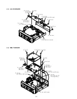
Page 20: ... out tray Refer to the item 2 6 4 Screws 5 Front panel block assembly 2 Tray ornament assembly 3 Flat cable From CN601 on MB 78 board 3 Connector From CN205 on AU 199 board Upper case Remove it up vertically Front panel 1 Screws case 3 TP2 1 Screws case 3 TP2 1 Screws case 3 TP2 2 Upper case 2 2 FRONT PANEL BLOCK ASSEMBLY ...

Page 21: ...board 6 BVTP3 10 3 BVTP3 10 4 Rear Panel 5 Flat cable From CN203 on AU 199 board 3 Shield plate 2 Screws 1Connector From CN002 on MB 78 board 1 Connector From CN001 on MB 78 board 8 MB 78 board 1 Flat cable From CN601 on MB 78 board 2 Screws 6 Screws 7 Lock hinge 1 Connector From CN361 on MB 78 board 1 Flat cable From CN301 on MB 78 board 5 Flat cable From CN101 252 302 452 on MB 78 board 4 Open M...

Page 22: ...onnector From CN201 on TK 47 board 5 Flexible board From CN001 on TK 47 board 5 Flexible board From CN002 on TK 47 board 7 TK 47 board 5 Connector From CN004 on TK 47 board 6 BVTP3 10 Release the stopper of tray by pushing hook 1 Screws 2 Press pulley bracket 3 Turn cam gear in the arrow A direction 5 Tray 4 A ...

Page 23: ... board CN001 Optical device KHS 180A J1N 8 820 005 02 Skew motor assembly X 3947 138 1 Sled motor assembly X 3947 137 1 KU160 SKEW DET 8 749 013 33 DC motor SPINDLE 1 698 944 11 Sled motor assembly X 3947 137 1 Optical device KHS 180A J1N 8 820 005 02 DC motor SPINDLE 1 698 944 11 Motor LOADING 1 698 942 21 ...

Page 24: ... 5E 2 9 CIRCUIT BOARDS LOCATION MB 78 VIDEO SERVO SYSTEM CONTROL AUDIO FL 90 DISPLAY OPERATION SWITCHES AU 199 VIDEO AUDIO INPUT OUTPUT POWER BLOCK FG 43 SLED MOTOR TK 47 RF SERVO HP 98 PHONES LE 21 LED ...

Page 25: ... DAC LRCK 8 YC0 7 IC251 DNR IC208 8 Y0 7 8 C0 7 SOG3 SCKG3 V SYNC H SYNC OH SYNC MRST 13 5M V SYNC H SYNC VSI SOG2 AVCK IC252 VIDEO ENCODER PLL IC209 R G B 27M VE ACLK IC205 IC206 IC204 IC206 IC206 27M DNR IC205 SCKG3 SOG3 DAC RST OSD IC207 V SYNC H SYNC SCLK SO 13 5M R G B M RST IC204 IC351 VIDEO AMP BOARD HP 98 IC215 AUDIO D A OPTICAL DIGITAL OUT VIDEO OUT R IC352 SOG3 SCKG3 DAC DATA DAC BCK DAC...

Page 26: ... BOARD CN501 CN301 HA HA HB HB VH VH SLD MT SLD MT 10 8 5 7 12 14 IC502 2 LD MT LD MT W OUT V OUT U OUT SP VH SP VH W IN2 W IN1 V IN2 V IN1 U IN2 U IN1 CN302 DVD TRK DVD TRK DVD FCS DVD FCS CD TRK CD TRK CD FCS CD FCS FROM SYSCON BLOCK TOFC IC804 141 CD DVD IC804 4 HFG IC805 97 NST IC804 7 SPCTL0 IC804 9 SPCTL1 IC804 8 SPGC1 IC804 22 SPGC2 IC804 10 OPN CLS IC804 5 S12V OFF IC804 19 TRAY FREE IC804...

Page 27: ... 100 SYS CLK 56 FL207 8 VSI IC804 37 SOG2 IC805 110 AVCK IC804 114 VCS IC804 36 XRST 93 H SYNC 98 VH SYNC 97 DCLKI 100 XCS 29 XSCLK 30 SDI 31 BI0 9 Y0 7 C0 7 19 22 24 27 33 36 38 41 PD8 PD15 PD0 PD7 FID 14 IC252 VIDEO ENCODER 64 Y OUT 58 C OUT 56 CP OUT XRST 10 V SYNC 15 PDCLK 11 H SYNC 16 SYS CLK 8 SO 48 VS IC804 152 SI 47 SCK 45 XCS 44 FL210 2 3 IC206 IC206 XT1 XT2 SO IC807 55 MRST IC805 54 SCLK...

Page 28: ...75 HA21 HA0 HA7 HD0 HD7 HA19 HA20 HA21 8 11 4 3 2 42 34 13 15 17 21 DQ0 DQ15 17 15 19 21 24 26 28 30 18 16 20 22 25 27 29 31 I O0 I O7 A0 A18 16 IC802 1M SRAM 8 17 1 IRQ6 29 WE 24 DE 22 CE1 30 CE2 12 CE 43 WE 14 OE 19 16 IC803 8M FLASH 74 XWR 73 XRD 8 HA0 HA8 9 11 14 16 19 64 1 8 3 5 63 HD0 HD7 OE 29 DIR 28 IA0 8 41 36 33 IA0 IA8 38 9 53 50 44 52 ID0 ID7 IC807 S G A 61 CK 55 SDO 56 SCLK 57 CG CS0 ...

Page 29: ...12 16 19 2 5 6 9 4 A19 C 11 9 ALE 8 AD0 7 19 20 13 8 A0 A7 OE 32 CE 30 7 1 2 IC602 IC603 4M PROM D0 D7 A8 A18 10 OE A8 A18 10 11 12 16 17 15 5 6 8 CN601 SCLK FLCS AD4 AD6 AD3 CW CCW IR FL 90 BOARD 10 11 12 16 17 15 5 6 8 CN102 15 32 35 S1 S19 IC101 DISPLAY DRIVER 47 DVD 48 VCD 49 CD SI 6 SCLK 8 FLS 9 50 JOG 43 38 REMOTE CONTROL RECEIVER REG 5V POWER S115 OPEN CLOSE S111 PLAY S1108 AMS PREV S106 AM...

Page 30: ...C202 FL201 VCC 7 VCC 13 VCC 25 VCC 38 VCC 44 CN001 VCC 14 IC101 VCC 13 DECRYRT VCC 33 VCC 53 VCC 73 IC811 FL803 VDD 1 IC804 L G A FL801 VDD 20 VDD 40 VDD 81 VDD 100 VDD 120 S12V OFF 19 VCC 2 IC801 EEPROM FL807 VCC 23 IC803 8M FLASH VCC 15 IC805 SYSTEM uCOM VCC 32 IC802 1M SRAM VCC 43 VCC 70 VCC VPP 77 VCC 83 VCC 84 AVCC 85 AVREF 86 VCC 99 VDD 13 9 IC807 S G A FL802 VDD 13 21 VDD 13 26 VDD 13 31 VD...

Page 31: ...damaged by the heat Some chip part will be indicated as follows Example C541 L452 22U 10UH TA A 2520 Constants of resistors capacitors ICs and etc with XX indicate that they are not used In such cases the unused circuits may be indicated All variable and adjustable resistors have characteristic curve B unless otherwise noted Signal name XEDIT EDIT PB XREC PB REC 2 non flammable resistor 1 fusible ...

Page 32: ......

Page 33: ...DVP M35 TK 47 RF SERVO SCHEMATIC DIAGRAM Ref No TK 47 Board 3 000 Series 4 7 4 8 4 9 RF SERVO TK 47 DVP M35 ...

Page 34: ......

Page 35: ...DVP M35 MB 78 DSP SCHEMATIC DIAGRAM Ref No MB 78 Board 1 000 Series 1 CN451 3 DVD 2 CN451 1 CD 3 IC506 DVD CD 0 2V div 0 2µsec div 0 5V div 0 1µsec div 27MHz 5 4Vp p 4 17 4 18 4 19 DSP MB 78 1 8 ...

Page 36: ...DVP M35 MB 78 AV DECODER SCHEMATIC DIAGRAM Ref No MB 78 Board 1 000 Series See page 4 13 for MB 78 BOARD printed wiring board 4 20 4 21 4 22 AV DECODER MB 78 2 8 ...

Page 37: ...B 78 BOARD printed wiring board 4 IC203 DVD 5 IC209 1 DVD CD 6 IC207 DVD 1V div 50µsec div 27MHz 5Vp p 1 4Vp p 60Hz 7 IC207 DVD 5Vp p 30Hz 8 IC252 8 5 4Vp p 27MHz 9 IC252 DVD 5Vp p 60Hz º IC252 5Vp p H IC252 DVD 1 2Vp p H IC252 DVD 0 9Vp p H IC252 DVD 1Vp p H 4 23 4 24 4 25 VIDEO ENCODER MB 78 3 8 ...

Page 38: ...RFACE SCHEMATIC DIAGRAM Ref No MB 78 Board 1 000 Series See page 4 13 for MB 78 BOARD printed wiring board IC303 ª DVD IC604 DVD CD 5 8Vp p 4MHz 4Vp p 7µsec IC303 ª CD 2 5Vp p 11 9µsec 4 26 4 27 4 28 INTERFACE MB 78 4 8 ...

Page 39: ...DVP M35 MB 78 MOTOR DRIVE SCHEMATIC DIAGRAM Ref No MB 78 Board 1 000 Series See page 4 13 for MB 78 BOARD printed wiring board 4 29 4 30 MOTOR DRIVE MB 78 5 8 ...

Page 40: ...DVP M35 MB 78 POWER SUPPLY SCHEMATIC DIAGRAM Ref No MB 78 Board 1 000 Series See page 4 13 for MB 78 BOARD printed wiring board 4 31 4 32 POWER SUPPLY MB 78 6 8 ...

Page 41: ...ries See page 4 13 for MB 78 BOARD printed wiring board IC806 DVD IC806 º DVD CD IC806 CD 56µsec 3 375MHz 1V div 0 2µsec div 2 5Vp p 106 ª IC806 122 º IC806 ª DVD IC805 DVD CD 3 3Vp p 5 4Vp p 27MHz 2V div 0 1µsec div 5 4Vp p 20MHz 4 33 4 34 4 35 4 36 DIGITAL PROCESS 1 MB 78 7 8 ...

Page 42: ...DVP M35 MB 78 DIGITAL PROCESS 2 SCHEMATIC DIAGRAM Ref No MB 78 Board 1 000 Series See page 4 13 for MB 78 BOARD printed wiring board 4 37 4 38 4 39 4 40 DIGITAL PROCESS 2 MB 78 8 8 ...

Page 43: ......

Page 44: ...DVP M35 AU 199 VIDEO AUDIO INPUT OUTPUT SCHEMATIC DIAGRAM Ref No AU 199 Board 2 000 Series 4 44 4 45 4 46 VIDEO AUDIO INPUT OUTPUT AU 199 ...

Page 45: ......

Page 46: ......

Page 47: ...DVP M35 FL 90 DISPLAY OPERATION SWITCHES LE 21 LED SCHEMATIC DIAGRAM Ref No FL 90 Board LE 21 Board 2 000 Series 4 51 4 52 DISPLAY OPERATION SWITCHES LED FL 90 LE 21 ...

Page 48: ......

Page 49: ...µF 250V R101 470K 1 2W C102 0 1µF 250V L101 18mH 0 5A C116 0 01µF 50V R116 220 2W T101 D511 S2L20U D611 D3S4M D311 D3S4M D211 S2L20U 1 2 3 4 5 6 7 8 9 10 11 12 13 14 15 1 2 3 5 2V 5 2V GND 3 3V GND E 5V GND P CONT AU 12V AU GND AU 12V 12V GND MTR 12V MTR GND R306 1 5K R305 330 R304 1 5K L511 10µH 2 6A C512 47µF 35V C511 1000µF 25V L311 10µH 2 6A L211 10µH 2 6A C513 47µF 35V R512 10K P511 60V 750mA...

Page 50: ......

Page 51: ...60 CNP901 AC IN CN101 F101 250V 2A C101 0 1µF 250V R101 470K 1 2W C102 0 1µF 250V L101 18mH 0 5A L102 18mH 0 5A C116 0 01µF 50V R116 220 1 2W T101 D511 S2L20U D611 D3S4M D311 D3S4M D211 S2L20U 1 2 3 4 5 6 7 8 9 10 11 12 13 14 15 5 2V 5 2V GND 3 3V GND E 5V GND P CONT AU 12V AU GND AU 12V 12V GND MTR 12V MTR GND R306 1 5K R305 330 R304 1 5K L511 10µH 2 6A C512 47µF 35V C511 1000µF 25V L311 10µH 2 6...

Page 52: ...R key in all modes except the middle of testing 5 2 System Control Diagnosis Press the 0 key while the initial menu is being displayed and enter the diagnosis mode The following display appears Use the adjustment remote commander RMT D102E 1 475 686 31 RMT D101J 1 475 219 11 21 and RMT D100E U 1 475 086 31 51 can also be used Syscon Diagnosis IF con Ver 1 220 9315 SYScon Ver 1 000 0000 Model NO DP...
Page 53: ...ommander microprocessor When the first digit is entered the item selection submenu appears Enter the remaining three digits and press ENTER When an item is selected the detailed test is performed When RAM test is selected the selected RAM is tested twice after changing data of all addresses Example Select the item 2 2 ROM Check Input 0202 because the item number is 2 2 Syscon Diagnosis IF con Ver ...

Page 54: ...ff f00 fff 1400 14ff address Test is executed sequentially from the top of the check item list of the diagnosis If errors which require visual inspection do not occur the system advances to the next test step W hen errors occur press the PREV key to repeat checking When errors occur or confirmation is necessary press the PREV key to repeat checking of the specified item Press NEXT to advance to th...

Page 55: ...k EURO model only 8 10 Y C output check EURO model only 8 11 RGB output check EURO model only 8 12 AV CONT Wide Mode check EURO model only 8 13 AV CONT Through check EURO model only 9 Audio related items 9 2 Sampling frequency 44 1 kHz 9 3 Sampling frequency 48 kHz 9 4 Sampling frequency 96 kHz 9 5 Audio digital output 9 6 Audio digital mute 9 7 MPEG audio analog output 9 8 Dual DAC serial 9 9 Aud...

Page 56: ... buffer Because all processings are performed within this function DAM is used for all processings including data transfer with the stack area When the more detailed check is selected all areas are checked twice using the inverted data However when one block is checked the succeeding four blocks are not checked in the simple check The check using the inverted data is also not performed in the simp...

Page 57: ...n Revision data reading Error 04 Data read error 13 DSP Data Ready cannot be not set In the masked ROM version data downloading cannot be executed Perform the data downloading in the ROM version only ROM or RAM is identified using the DBUSY signal of DSP The unique downloading flat is prepared in this diagnosis This flat is 0 when data is not downloaded and is 1 when already downloaded Error is as...

Page 58: ...eement check is performed for confirmation 6 4 ARP DRAM ROM Data ARP DRAM ARP reading and check if data agrees Error 03 Data write error ARP cannot be set into Write Enable 04 Data read error ARP cannot be set into Read Enable 05 Write data and read data do not agree In this test the ROM pattern is copied to the entire area to be checked During this copying address of the copy source ROM is return...

Page 59: ...he data of 0 1 2 3 4 has already been written for this check This data is checked if the read out data agree with this data at every interrupt into the respective sectors If write data and read data do not agree check can be repeated 7 AV decoder 7 2 64020 64021 register Write into register Read from register and check if data agree Error 05 Write data and read data do not agree The 51 registers t...

Page 60: ... DMA transfer address error 10 Data transfer error between chips This check is performed as follows The AC 3 audio data that is stored in ROM is written first Check if the data is transferred to the AV decoder If the transfer error is not detected the target address of AV decoder to which the transfer data is written A part of the data that is transferred to the AV decoder is sent to the SH RAM us...

Page 61: ...ata every pixel The color difference signals of Cr and Cb are set to 80h which is B W signal and turn the display to on Then the color difference signals are written while changing data every line Because both of luminance and color difference signals are the regular pattern the processing speed is increased by transferring the repetition data by DMA When the detailed check mode is selected the co...

Page 62: ...the AV CONT H E V Y L and E V RGB H Color bar is output in the same way as 8 2 8 11 RGB output check EURO model only Color bar output from NTSC encoder Error 11 Serial transfer error Video signal is output by setting the AV CONT H E V Y H and E V RGB H Color bar is output in the same way as 8 2 8 12 AV CONT Wide Mode check EURO model only Color bar output from NTSC encoder Error 11 Serial transfer...

Page 63: ...stream of AC 3 Audio that is stored in ROM is sent to the AV decoder through ARP and is output to Digital Audio I F At this time the mute signal is turned on and off every other time four times then is output First time Mute OFF Sound can be heard Second time Mute ON Sound cannot be heard Third time Mute OFF Sound can be heard Fourth time Mute ON Sound cannot be heard When error is not detected a ...

Page 64: ...e has significantly the lower level around 48dB When error is not detected a message is output which prompts key input This check is performed in the DD machines and KARAOKE machines only 9 11 MGA DCS selector switch check DD machines only ROM audio data ARP AVD MGA Analog Audio Out Error 10 Data transfer from ARP to AV decoder is not possible 35 2 ch DAC serial transfer interrupt is not detected ...

Page 65: ...he diagnosis test program works correctly or not This test is performed by downloading the test program The test program abcde is written to the AC 3 decoder address 0478d Check that the data which has already been written to the address 0478d from host is re written to abcde when the diagnosis program is downloaded The machine is set to the test tone input mode in order to download the test progr...

Page 66: ...nt to AV decoder through ARP The decoded audio data is output from AC 3 DAC in the form of analog through DIR and AC 3 DSPs When error is not detected a message is output which prompts key input 10 8 Analog gain switch check AC 3 DSP test tone AC3 DAC Audio Out Analog Gain On Off Error 43 AC3 DAC For main output serial transfer interrupt is not detected 44 AC3 DAC For center output serial transfer...

Page 67: ...E DSP CXD2721Q interrupt is not detected 62 KARAOKE DSP does not become ready This test is performed by writing 0x000fef to the KARAOKE DSP setup register address 0x00 and checks if the address is initialized to 0x000010 by reset pulse 11 4 KARAOKE DSP serial ROM audio data ARP AVD KARAOKE DSP AOUT Key control Error 10 Data transfer from ARP to AV decoder is not possible 35 2 ch DAC serial transfe...

Page 68: ...transfer error between chips 11 Serial transfer error 12 EEPROM does not become ready 13 Data Ready cannot be not set 14 DSP download error 21 ARP interrupt is not detected 22 Decrypt interrupt is not detected 31 AVS decoder interrupt is not detected 32 Servo DSP interrupt is not detected 33 SSI interrupt is not detected 34 DNR interrupt is not detected 35 2 ch DAC interrupt is not detected 36 EEP...

Page 69: ...e emergency codes When the key either 0 or 1 or 2 or 3 of remote commander is pressed the confirmation message appears as shown below When you agree with the message press ENTER and automatic adjustment starts Another item number can be selected by pressing the desired item number if ENTER is not pressed yet Automatic adjustment can be stopped and return to the initial menu at any time when you pr...

Page 70: ...uto Tracking Gain Auto EQ Servo Stop Auto Loop Filter Offset Go To Home position Pull in Memory Jitter Check LD ON Servo Stop Spindle Start Search Check Tilt ON Focus ON FOK Check Tangential screw adjustment Make this adjustment only when the pickup was replaced As for adjustment rotate the T SKEW adjusting screw on the pickup so that the displayed jitter becomes minimum CCW makes jitter smaller A...

Page 71: ...yer disc When 3 DVD Dual Layer Disc is selected and the DVD dual layer disc is inserted the adjustment is performed in the order described below The adjustment values of each layer are saved in EEPROM DVD dual layer adjustment procedure Layer 0 LD ON Spindle Start Layer 1 Tilt ON Focus Jump L0 L1 Focus ON FOK Check FOK Check Sled Move Sled ON Auto Tracking Offset CLVA FOK Check Lock Check Layer Ch...

Page 72: ...eturn button Returns to Drive Manual Operation Set Up SET UP button After stopping the machine returns to the Test Mode Menu Eject Loading Open Close button Stop Eject Loading CLEAR CLEAR button Moving between the menu s submodes Ten key 0 to 9 button Selection of menu Cursor key button Increasing the Manual Adjust values Cursor key button Decreasing the Manual Adjust values 5 4 1 Setup Displays I...

Page 73: ... of CD is displayed If it is not displayed spindle servo fails to lock and the machine is faulty When the spindle system is faulty or when RF signal is not picked up the spindle can run away In such a case do not operate CLVA 0 LD Turns on and off the laser power 1 SP Turns on and off the spindle system When the spindle is turned on it enter the constant speed mode 2 Tilt Turns on and off the tilt...

Page 74: ...tatus is established 6 Chuck Chucking is performed 7 Skip The disc position is skipped 5 4 4 Manual Control 3 Open and close can be executed using the Open Close button Chucking is not executed by close Operate to chuck afer closed Manual Control 3 SA 0364AD SI 00 ENG 00 0 FWD 32TJ 6 FJ0 1 1 RVS 32TJ 7 FJ1 0 2 FWD 500TJ 8 Li0 1 3 RVS 500TJ 9 LJ1 0 4 FWD 10kTJ FWD 1TJ 5 RVS 10kTJ RVS 1TJ DVD SL 12c...

Page 75: ... 0 TRK Offset The tracking offset adjustment is performed When adjusting a DVD the tracking offset is canceled coarsely by SSI33P3720A with the peak bottom that is measured by DSP The fine tracking offset adjustment is performed within the DSP This adjustment sets the value for the fine adjustment Because this is the adjustment within the DSP only the DC component of the tracking traverse is not c...

Page 76: ...fset It performs the automatic adjustment of Tracking Offset The adjustment value is stored in EEPROM Perform this adjustment with the player in Focus and and with Tracking Off Because pickup moves toward outer circumference in this adjustment do not perform this adjustment in outer circumference In the case of CD adjustment the simple AGC adjustment of tracking is also performed in this adjustmen...

Page 77: ... cleared and lost It is recommended to take note of the former setting values before performing this item 6 EEPROM Data The setting data of EEPROM is listed as shown below the data is hexadecimal notation of 00 to FF When you want to return to the original check display press 6 EEPROM Data CD DVD ID no 00 SL L0 L1 Focus Offset Focus Gain TRK Offset TRK CONT TRK Gain Tilt Offset pullin Level EQ Boo...

Page 78: ...mation is displayed on four pages Move to the next page or previous page using the key and the key Return to the initial menu by pressing the RETURN key EMG Hist Page 01 CD 000000 Hour 1 00 00 00 00 00 00 00 00 00 00 00 00 2 00 00 00 00 00 00 00 00 00 00 00 00 Page Up Exit Return EMG Hist Page 02 DVD 000000 Hour 3 00 00 00 00 00 00 00 00 00 00 00 00 4 00 00 00 00 00 00 00 00 00 00 00 00 Page Up Pa...

Page 79: ... is completed How to clear the history of emergencies Press the keys of remote commander in the order of TITLE and CLEAR Display of the history of emergencies is changed to 00 How to clear pre set of the system control Press the keys of remote commander in the order of DVD MENU and CLEAR The message Clear User preset flashes for about 3 seconds Clearing pre set can be canceled by stopping the STOP...

Page 80: ...rol requests address that does not exist 71 System control requests time code that is not used 72 System control requests track No that is not used 73 The lock in operation is not completed within the specified number of times 8x Data related items 80 Continuity of address has abnormality DVD 81 Cannot read address even retry is executed CD 82 TOC read is not completed within the specified period ...

Page 81: ...F Balance 62 Adjust Jitter Gain 63 TOC Control Data Read 70 Spin Down 80 Seek 90 Error Recovery A0 Service A1 Nop For Service F0 Exception processing 1 F1 Exception processing 2 F2 Exception processing 3 F3 Exception processing 4 F4 Exception processing 5 FE Changing modes is completed FF Invalid Code Mode is not changed 5 8 3 Disc Status Table History of emergencies No EMG MECHA DISC MODE ERR2 ER...

Page 82: ...J 6090 069 A single layer In making adjustment refer to 6 4 Adjustment Related Parts Arrangement 6 1 POWER SUPPLY CHECK MB 78 board Mode E E Instrument Digital Voltmeter EVER 5 3V Check Measurement Point CN001 pin 3 Specification 5 4 0 2V REG 3 3V Check Point CN001 pin 5 Specification 3 3 0 2V REG 5 2V Check Point CN001 pins 7 8 Specification 5 2 0 2V M 12V Check Point CN002 pin 2 Specification 12...

Page 83: ...ars Test point J354 LINE OUT VIDEO Terminating 75Ω Instrument Oscilloscope Adjusting element RV251 Specification 1 0 02 Vp p Adjusting method 1 In the test mode initial menu 0 Syscon Diagnosis set so that CXD1914 color bars are generated 2 Adjust the RV251 to attain 1 0 02 Vp p Fig 6 2 2 S terminal Output Check AU 199 board Purpose Check S terminal video output If it is incorrect pictures will not...

Page 84: ...1914 Serial check in test mode menu 0 Syscon Diagnosis 8 2 Signal Color bars Test point J354 LINE OUT VIDEO Terminating 75Ω Instrument Oscilloscope Specification 1 0 05 Vp p Checking method 1 Confirm that the Y level is 1 0 05 Vp p Fig 6 7 4 Checking S Video Output S C AU 199 board Purpose This checks whether the S C satisfies the NTSC Standard If it is not correct the colors will be too dark or l...

Page 85: ... 17 18 19 16 not supplied Included in No 11 Ref No Part No Description Remarks Ref No Part No Description Remarks 1 3 945 284 41 KNOB VOLUME 2 3 988 015 31 RING SHUTTLE 3 X 3948 391 1 ORNAMENT ASSY TRAY 4 X 3948 400 2 PANEL ASSY FRONT 5 A 6065 068 A LE 21 BOARD COMPLETE 6 A 6065 067 A FL 90 BOARD COMPLETE 7 4 951 620 01 SCREW 2 6X8 BVTP 8 3 363 099 01 SCREW CASE 3 TP2 9 3 988 052 01 CASE UPPER 10 ...

Page 86: ...55 1 468 287 21 POWER BLOCK HS 930SH EXCEPT E 55 1 468 287 31 POWER BLOCK HS 930SF E 56 4 965 822 01 FOOT 57 A 6065 066 A AU 199 BOARD COMPLETE 58 1 783 339 11 CABLE FLAT FMT 21 59 1 783 343 11 CABLE FLAT FMA 4 60 3 646 090 11 RIVET NYLON 61 3 691 950 01 SPACER P C BOARD 62 3 703 150 11 CLAMP 63 3 975 023 01 SCREW CUSHION STOPPER 64 1 782 001 61 CORD POWER EXCEPT CN 64 1 782 692 31 CORD POWER CN 6...

Page 87: ...53 3 975 087 01 GEAR DRIVE 154 3 975 086 01 GEAR TRAY DRIVING 155 3 975 072 01 GEAR LOADING MIDWAY 156 3 975 071 01 PULLEY LOADING 157 3 669 596 00 WASHER 2 3 STOPPER 158 3 975 070 01 BELT 159 3 975 085 01 PULLEY MOTOR 160 3 975 089 01 BRACKET PRESS PULLEY 161 3 975 074 01 PULLEY PRESS 162 3 975 077 01 SCREW BU STOPPER 163 3 975 088 03 HOLDER BASE UNIT 164 X 3948 398 1 HOLDER ASSY MD 165 A 6065 06...

Page 88: ...AL KHS 180A J1N 208 1 665 390 11 OP 15 FLEXIBLE BOARD 209 3 975 067 01 GEAR RACK 210 3 975 064 01 RETAINER SLED GEAR 211 A 6065 078 A FG 43 A COMPL BOARD COMPLETE 213 3 975 059 01 RETAINER SKEW GEAR 214 3 975 057 01 GEAR SKEW 215 4 974 711 01 SCREW 2X5 P TYIGHT PTTWH 216 4 974 725 01 SCREW M1 7X2 5 P 218 A 4683 008 A GEAR ASSY LIMITTER 219 4 974 720 01 GEAR S B 220 4 974 726 01 GEAR S A 221 1 783 ...

Page 89: ...LM 0 1uF 5 63V C290 1 117 793 11 MYLAR 330PF 5 50V C291 1 117 793 11 MYLAR 330PF 5 50V C298 1 164 232 11 CERAMIC CHIP 0 01uF 50V C299 1 124 589 11 ELECT 47uF 20 16V C300 1 164 232 11 CERAMIC CHIP 0 01uF 50V C301 1 124 261 00 ELECT 10uF 20 50V C302 1 124 589 11 ELECT 47uF 20 16V C303 1 163 231 11 CERAMIC CHIP 15PF 5 50V C304 1 163 243 11 CERAMIC CHIP 47PF 5 50V C305 1 163 243 11 CERAMIC CHIP 47PF 5...

Page 90: ...16 109 00 METAL CHIP 330K 5 1 10W R236 1 216 109 00 METAL CHIP 330K 5 1 10W R241 1 216 041 00 METAL CHIP 470 5 1 10W R242 1 216 041 00 METAL CHIP 470 5 1 10W R249 1 216 073 00 METAL CHIP 10K 5 1 10W R250 1 216 097 91 RES CHIP 100K 5 1 10W R254 1 208 805 11 RES CHIP 9 1K 0 50 1 10W R255 1 216 049 91 RES CHIP 1K 5 1 10W R258 1 216 049 91 RES CHIP 1K 5 1 10W R262 1 216 296 91 SHORT 0 R269 1 216 097 9...

Page 91: ...08 974 21 INDUCTOR 22uH FLUORESCENT INDICATOR ND101 1 517 714 11 INDICATOR TUBE FLUORESCENT TRANSISTOR Q105 8 729 424 08 TRANSISTOR UN2111 Q106 8 729 105 29 TRANSISTOR 2SA1385 Q107 8 729 216 22 TRANSISTOR 2SA1162 RESISTOR R103 1 216 037 00 METAL CHIP 330 5 1 10W R104 1 216 073 00 METAL CHIP 10K 5 1 10W R105 1 216 073 00 METAL CHIP 10K 5 1 10W R106 1 216 073 00 METAL CHIP 10K 5 1 10W R107 1 216 073...

Page 92: ...TOR 2SD2114KT146 Q002 8 729 023 22 TRANSISTOR 2SD2114KT146 RESISTOR R001 1 216 029 00 METAL CHIP 150 5 1 10W R002 1 216 029 00 METAL CHIP 150 5 1 10W R003 1 216 089 91 RES CHIP 47K 5 1 10W R004 1 216 089 91 RES CHIP 47K 5 1 10W R005 1 216 081 00 METAL CHIP 22K 5 1 10W R006 1 216 081 00 METAL CHIP 22K 5 1 10W R007 1 216 049 91 RES CHIP 1K 5 1 10W R008 1 216 049 91 RES CHIP 1K 5 1 10W R009 1 216 049...

Page 93: ... 16V C269 1 162 970 11 CERAMIC CHIP 0 01uF 10 25V C270 1 162 917 11 CERAMIC CHIP 15PF 5 50V C271 1 162 917 11 CERAMIC CHIP 15PF 5 50V C272 1 162 917 11 CERAMIC CHIP 15PF 5 50V C282 1 107 826 11 CERAMIC CHIP 0 1uF 10 16V C301 1 162 967 11 CERAMIC CHIP 0 0033uF 10 50V C303 1 126 193 11 ELECT 1uF 20 50V C304 1 162 967 11 CERAMIC CHIP 0 0033uF 10 50V C305 1 165 176 11 CERAMIC CHIP 0 047uF 10 16V C306 ...

Page 94: ...1 CERAMIC CHIP 0 1uF 10 16V C552 1 124 778 00 ELECT CHIP 22uF 20 6 3V C553 1 162 969 11 CERAMIC CHIP 0 0068uF 10 25V C554 1 162 969 11 CERAMIC CHIP 0 0068uF 10 25V C555 1 162 970 11 CERAMIC CHIP 0 01uF 10 25V C556 1 162 970 11 CERAMIC CHIP 0 01uF 10 25V C558 1 164 489 11 CERAMIC CHIP 0 22uF 10 16V C559 1 162 970 11 CERAMIC CHIP 0 01uF 10 25V C560 1 162 970 11 CERAMIC CHIP 0 01uF 10 25V C561 1 162 ...

Page 95: ...CONNECTOR 1 5MM SMD 5P CN452 1 784 326 11 CONNECTOR FFC 27P CN601 1 784 685 11 CONNECTOR FFC FPC 20P CN801 1 573 806 21 PIN CONNECTOR 1 5MM SMD 6P TRIMMER CT201 1 141 422 11 CAP ADJ 10PF DIODE D002 8 719 975 40 DIODE RB411D D101 8 719 988 62 DIODE 1SS355 D102 8 719 988 62 DIODE 1SS355 D103 8 719 988 62 DIODE 1SS355 D502 8 719 988 62 DIODE 1SS355 D801 8 719 988 62 DIODE 1SS355 D802 8 719 048 98 DIO...

Page 96: ...BM29F800B 90PF IC804 8 759 525 66 IC CXD8728Q IC805 8 759 489 89 IC HD6437034AD49F IC806 8 759 522 09 IC CXD1865R IC807 8 759 526 79 IC CXD8747Q IC810 8 759 525 65 IC uPD424260ALG5 A70 7JF IC811 8 752 390 59 IC CXD1904Q IC812 8 759 486 55 IC NJM2370U33 TE2 IC SOCKET ICS803 1 251 496 21 SOCKET IC COIL L001 1 409 529 41 INDUCTOR 0uH L002 1 409 529 41 INDUCTOR 0uH L004 1 409 529 41 INDUCTOR 0uH L005 ...

Page 97: ...0 1 216 809 11 METAL CHIP 100 5 1 16W R231 1 216 809 11 METAL CHIP 100 5 1 16W R232 1 216 845 11 METAL CHIP 100K 5 1 16W R235 1 216 864 11 METAL CHIP 0 5 1 16W R236 1 216 809 11 METAL CHIP 100 5 1 16W R237 1 216 809 11 METAL CHIP 100 5 1 16W R238 1 216 809 11 METAL CHIP 100 5 1 16W R239 1 216 809 11 METAL CHIP 100 5 1 16W R240 1 216 805 11 METAL CHIP 47 5 1 16W R241 1 216 805 11 METAL CHIP 47 5 1 ...

Page 98: ...CHIP 0 5 1 16W R393 1 216 797 11 METAL CHIP 10 5 1 16W R394 1 216 797 11 METAL CHIP 10 5 1 16W R395 1 216 797 11 METAL CHIP 10 5 1 16W R396 1 216 797 11 METAL CHIP 10 5 1 16W R397 1 216 837 11 METAL CHIP 22K 5 1 16W R398 1 216 837 11 METAL CHIP 22K 5 1 16W R399 1 216 797 11 METAL CHIP 10 5 1 16W R400 1 216 797 11 METAL CHIP 10 5 1 16W R401 1 216 797 11 METAL CHIP 10 5 1 16W R402 1 216 797 11 METAL...

Page 99: ...15K 5 1 16W R580 1 216 809 11 METAL CHIP 100 5 1 16W R582 1 216 864 11 METAL CHIP 0 5 1 16W R583 1 216 809 11 METAL CHIP 100 5 1 16W R584 1 216 809 11 METAL CHIP 100 5 1 16W R585 1 216 821 11 METAL CHIP 1K 5 1 16W R586 1 216 833 11 METAL CHIP 10K 5 1 16W R587 1 216 809 11 METAL CHIP 100 5 1 16W R588 1 216 809 11 METAL CHIP 100 5 1 16W R592 1 216 845 11 METAL CHIP 100K 5 1 16W R593 1 216 835 11 MET...

Page 100: ... CHIP 100 5 1 16W R838 1 216 833 11 METAL CHIP 10K 5 1 16W R839 1 216 857 11 METAL CHIP 1M 5 1 16W R840 1 216 864 11 METAL CHIP 0 5 1 16W R842 1 216 801 11 METAL CHIP 22 5 1 16W R843 1 218 881 11 RES CHIP 27K 0 50 1 16W R844 1 218 847 11 RES CHIP 1K 0 50 1 16W R845 1 218 885 11 RES CHIP 39K 0 50 1 16W R847 1 216 833 11 METAL CHIP 10K 5 1 16W R848 1 216 864 11 METAL CHIP 0 5 1 16W R849 1 218 831 11...

Page 101: ...C056 1 107 725 11 CERAMIC CHIP 0 1uF 10 16V C058 1 124 779 00 ELECT CHIP 10uF 20 16V C059 1 163 009 11 CERAMIC CHIP 0 001uF 10 50V C060 1 163 989 11 CERAMIC CHIP 0 033uF 10 25V C061 1 163 989 11 CERAMIC CHIP 0 033uF 10 25V C062 1 124 779 00 ELECT CHIP 10uF 20 16V C064 1 124 779 00 ELECT CHIP 10uF 20 16V C065 1 109 982 11 CERAMIC CHIP 1uF 10 10V C066 1 164 232 11 CERAMIC CHIP 0 01uF 50V C067 1 163 ...

Page 102: ... 00 METAL CHIP 330K 5 1 10W R111 1 216 073 00 METAL CHIP 10K 5 1 10W R112 1 216 113 00 METAL CHIP 470K 5 1 10W R113 1 216 057 00 METAL CHIP 2 2K 5 1 10W R149 1 216 073 00 METAL CHIP 10K 5 1 10W R150 1 216 081 00 METAL CHIP 22K 5 1 10W R151 1 216 059 00 METAL CHIP 2 7K 5 1 10W R152 1 216 077 00 METAL CHIP 15K 5 1 10W R153 1 216 093 00 METAL CHIP 68K 5 1 10W R154 1 216 081 00 METAL CHIP 22K 5 1 10W ...

Page 103: ...930SF E Ref No 9 000 Series CAPACITOR C110 9 880 447 01 ELECT 270uF 400V C114 1 107 967 11 ELECT 1uF 400V C211 1 111 087 11 ELECT 330uF 35V C212 1 126 947 11 ELECT 47uF 35V C213 1 126 947 11 ELECT 47uF 35V C214 1 126 947 11 ELECT 47uF 35V C301 1 126 960 11 ELECT 1uF 50V C311 1 111 087 11 ELECT 330uF 35V C312 1 111 087 11 ELECT 330uF 35V C313 1 126 947 11 ELECT 47uF 35V C314 1 126 948 11 ELECT 100u...

Page 104: ...CN 207 8 820 005 02 DEVICE OPTICAL KHS 180A J1N 212 1 783 341 11 CABLE FLAT FMF 28 FAN1 1 698 792 11 FAN DC M501 X 3947 137 1 MOTOR ASSY SLED M901 1 698 944 11 MOTOR DC SPINDLE M902 X 3947 138 1 MOTOR ASSY SKEW M903 1 698 942 21 MOTOR LOADING ACCESSORIES PACKING MATERIALS 1 569 008 11 ADAPTOR CONVERSION 2P E 1 575 334 11 CORD CONNECTION AV CONNECTION 1 5m 1 575 335 21 CORD CONNECTION S VIDEO 1 5m ...

Page 105: ...DVP M35 158 Sony Corporation Home A V Products Company 9 921 677 11 98C16096 1D Printed in Japan 1998 3 Published by General Engineering Dept Osaki East ...

Reviews: