


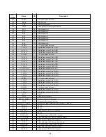


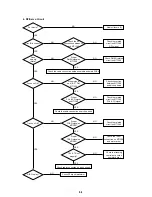
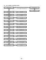


7-5
Pin
Name
I/O
Description
number
193
YUV0/CIN
O
Video data output bit 0 Compensation capacitor
194
FS
O
Full scale adjustment
195
VREF
O
Bandgap reference voltage
196
DACVDDC
-
3.3V power pin for VIDEO DAC circuitry
197
ASDATA0/GPO_2
I/O
Audio serial data 0 (Front-Left/Front-Right) DSD data left channel Trap value in power-
on reset
198
RVREF/GPIO_6
I/O
GPIO
199
RCLKB/GPIO_5
I/O
GPIO
200
GPIO_4
I/O
GPIO
201
GPIO_3
I/O
GPIO
202
ASDATA1/GPO_1
I/O
TP155
203
ASDATA2/GPO_2
I/O
TP152
204
SPMCLK
I/O
KEYSCAN C6
205
SPDATA
I/O
KEYSCAN C7
206
SPLRCK
I/O
ADAC MC
207
SPBCK
I/O
TP165
208
DVDD3
-
3.3V power pin for internal
209
ALRCK
I/O
Audio left/right channel clock Trap value in power-on reset: I) 1 : use external 373 II)
0: use internal 373
210
ABCK
O
Audio bit clock Phase de-modulation
211
ACLK
O
Audio DAC master clock
212
ASDATA3
I/O
TP152
213
DVDD18
-
1.8V power pin for internal
214
ASDATA4
I/O
TP151
215
MC_DATA
I/O
Inout PD SMT
216
SPDIF
O
SPDIF output
217
APLLVDD3
-
3.3V Power pin for audio clock circuitry
218
APLLCAP
O
APLL External
219
APLLVSS
-
Ground pin for audio clock circuitry
220
ADACVSS2
-
Ground pin for AUDIO DAC circuitry
221
ADACVSS1
-
Ground pin for AUDIO DAC circuitry
222
ARF (SW)
O
AUDIO DAC Sub-woofer channel output While internal AUDIO DAC not used: GPIO
223
ARS/SDATA3
O
TP149
224
AR/SDATA1
O
AUDIO DAC Right channel output While internal AUDIO DAC not used: a. SDATA1
225
AVCM
O
AUDIO DAC reference voltage
226
AL/SDATA2
O
AUDIO DAC Left Surround channel output While internal AUDIO DAC not used:
a. SDATA2
227
ALS/SDATA 0
O
TP148
228
ALF/(CTR)
O
TP147
229
ADACVDD1
-
3.3V power pin for AUDIO DAC circuitry
230
ADACVDD2
-
3.3V power pin for AUDIO DAC circuitry
231
RFGND18
-
Analog ground
232
RFVDD18
-
Analog power 1.8V
233
XTALO
O
27M crystal out
234
XTALI
I
27M crystal in
235
JITFO
O
The output terminal of RF jitter meter.
236
JITFN
I
The input terminal of RF jitter meter.
237
PLLVSS
-
Ground pin for data PLL and related analog circuitry.
Summary of Contents for DVP-FX850
Page 4: ... 4 MEMO ...
Page 18: ...2 2 2 2 TRAVERSE 1 traverse 2 hinge cosmetic ...
Page 22: ...DVP FX850 3 4E DVP FX850 MEMO ...
Page 38: ...DVP FX850 5 12E DVP FX850 MEMO ...
Page 50: ...7 8E MEMO ...
Page 52: ...8 2E MEMO ...
Page 64: ...REVISION HISTORY Ver Date Description of Revision 1 0 2007 05 New DVP FX850 ...


