background image

26

DVP-CX777ES

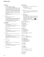
6. AV Decoder

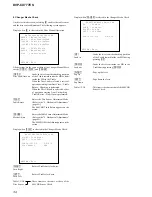
(6-2) 1935 RAM

Data write 

t

 read, and accord check

Error 14: AVD RAM read data discord
The program code data stored in ROM (IC106) are copied
to all areas of RAM (IC404, 405) connected to the AVD
(IC403) through the bus, then they are read and checked if
they accord. Further, the same test is conducted once again
with the data where all bits are inverted between 1 and 0. If
discord is detected, faulty address, written data, and read
data are displayed following the error code 14, and the test
is suspended.
During the test, OSD display becomes blank as the OSD
area is also checked.

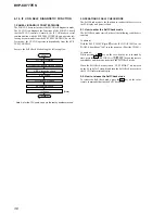
(6-3) 1935 SP

ROM 

t

 AVD RAM 

t

 Video OUT

Error: Not detected.
The data including sub picture streams in ROM (IC106)
are transferred to the RAM (IC404, 405) in AVD (IC403),
and output as video signals from the AVD (IC403).
Though OSD display becomes blank, the output of video
signals continues until the key is pressed.

7. Video Output

(7-2) Color Bar

AVD color bar command write 

t

 Video OUT

Error: Not detected.
The command is transferred to the AVD, and the color bar
signals are output from video terminals.

(7-3) Composite Out

AVD color bar command write 

t

 Video (Composite, Y/C)

OUT
Error: Not detected.
The command is transferred to the AVD, and the color bar
signals are output from video terminals.

(7-4) Y/C Out

AVD color bar command write 

 Video (Composite, Y/C)

OUT
Error: Not detected.
The command is transferred to the AVD, and the color bar
signals are output from video terminals.
They are output from all video terminals (Composite, Y/C,
Component).

(7-5) —————

Check no support.

(7-6) Component Out

AVD color bar command write 

t

 Video (Component, Y/

C) OUT
Error: Not detected.
The command is transferred to the AVD, and the color bar
signals are output from video terminals.

(7-7) —————

Check no support.

8. Audio Output

(8-2) ARP 

t

 1935

Data flow from supply system DRAM to SDRAM of AV
Decoder is tested.
Error 15: ARP 

t

 1935 video NG

16: ARP 

t

 1935 audio NG

(8-3) Audy

Register check of Audy (IC801) and SDRAM (IC802) check
are performed. After above checks are performed, transit
to the next test tone (8-4).

(8-4) Test Tone

Pink noise output
Error: Not detected.
In the models without DD output, the test tone is output
from L and R of 2-channel only, and in the models with
DD output, the test tone is output from L and R of 2-chan-
nel, and all channels of 5.1 output.
After turning on all outputs, each time the

>

key  is

pressed, the output channel is switched for individual chan-
nel checking.

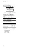
Diagnosis Check Items List

2. Version Display
(2-2) Revision
(2-3) ROM Check Sum
(2-4) Model Type
(2-5) Region
(2-6) M’t Check

3. Peripheral
(3-2) EEPROM Check
(3-3) Gate Array Check
(3-4) NAND FLASH Check
(3-5) SACD Check
(3-6) VENC Check
(3-7) ———— (Function not supported)
(3-8) EX RAM Check

4. Servo
(4-2) Servo DSP Check
(4-3) ———— (Function not supported)
(4-4) RF Amp (SSI) W/R Check

5. Data Supply System
(5-2) ARP Register Check
(5-3) ARP to RAM Data Bus
(5-4) ARP to RAM Address Bus
(5-5) ARP RAM Check

6. AV Decoder
(6-2) 1935 RAM
(6-3) 1935 SP

7. Video Output
(7-2) Color Bar
(7-3) Composite Out
(7-4) Y/C Out
(7-5) ———— (Function not supported)
(7-6) Component Out
(7-7) ———— (Function not supported)

8. Audio Output
(8-2) ARP 

t

 1935

(8-3) Audy
(8-4) Test Tone

Summary of Contents for DVP-CX777ES

Page 1: ... R 1 2 Phono jack 2 Vrms 10 kilohms DIGITAL OUT OPTICAL Optical output jack 18 dBm wave length 660 nm DIGITAL OUT COAXIAL Phono jack 0 5 Vp p 75 ohms 5 1CH OUTPUT Phono jack 2 Vrms 10 kilohms COMPONENT VIDEO OUT Y PB CB PR CR Phono jack Y 1 0 Vp p PB CB PR CR interlace 0 648 Vp p progressive or interlace 0 7 Vp p 75 ohms BLACK LEVEL is ON BLACK LEVEL is OFF LINE OUT VIDEO 1 2 Phono jack 1 0 Vp p 7...

Page 2: ...a soft cloth C 31 The disc is not inserted correctly Re insert the disc correctly C 32 The front cover automatically opens and the player enters standby mode Check that there is nothing wrong inside the rotary table such as a fallen disc After you have checked the inside of the rotary table and resolved any possible problems press H E XX xx is a number To prevent a malfunction the player has perfo...

Page 3: ...rly all battery operated digital multimeters that have a 2 V AC range are suitable See Fig A Fig A Using an AC voltmeter to check AC leakage 1 5 kΩ 0 15 µF AC voltmeter 0 75 V To Exposed Metal Parts on Set Earth Ground ATTENTION AU COMPOSANT AYANT RAPPORT À LA SÉCURITÉ LES COMPOSANTS IDENTIFIÉS PAR UNE MARQUE 0 SUR LES DIAGRAMMES SCHÉMATIQUES ET LA LISTE DES PIÈCES SONT CRITIQUES POUR LA SÉCURITÉ ...

Page 4: ...IDEO and DVD RW are trademarks Region code Your player has a region code printed on the back of the unit and will only play DVD VIDEOs playback only labeled with identical region codes This system is used to protect copyrights DVD VIDEOs labeled will also play on this player If you try to play any other DVD VIDEO the message Playback prohibited by area limitations will appear on the TV screen Depe...

Page 5: ...iagram MB Board 12 15 68 7 19 Schematic Diagram MB Board 13 15 69 7 20 Schematic Diagram MB Board 14 15 70 7 21 Schematic Diagram MB Board 15 15 71 7 22 Printed Wiring Board MB Board Component Side 72 7 23 Printed Wiring Board MB Board Conductor Side 73 TABLE OF CONTENTS 7 24 Printed Wiring Board DRIVER Board 74 7 25 Schematic Diagram DRIVER Board 75 7 26 Printed Wiring Boards MOTOR SWITCH Section...

Page 6: ... correctly Drive Auto Adjustment can t be performed In this case initialize Memory in the following procedures Procedure 1 Set the test mode See page 23 2 Press the 2 key of the remote commander and set the DRIVE MANUAL OPERATION See page 29 3 Press the 6 key of the remote commander and set the 2 6 Memory Check See page 32 4 Press the CLEAR key of the remote commander and initial ize Memory NOTES ...

Page 7: ... pulley assy Remove the pulley assy and clean the lens of optical pick up through this hole NOTE FOR INSTALLATION AV board AV board Front side MB board cables MB board to driver board sensor board cables MB board to driver board sensor board MB board AV board power block locking wire saddle MB board It takes care that the cables doesn t hang down cable AV board to panel L board cables MB board to ...

Page 8: ...oard AV board cables It is made to contact and for there not to be a power block and cables power block MB board power block driver board cables cables When installing the cables it is made to make it crawl in a chassis ...

Page 9: ...9 DVP CX777ES SERVICE POSITION MB board Optical pick up block MB board CN102 Connect the jig J 2501 086 A to MB board CN102 and panel L board CN1005 panel L board CN1005 optical pick up DVBU26 ...

Page 10: ...tton indicator O ENTER previous next enter dial P O RETURN button Q C X x c ENTER buttons R DISPLAY button S TOP MENU button T MENU button U VIDEO CONTROL button V SURROUND button W ONE ALL DISCS button X FOLDER button Y LOAD button Z remote sensor wj VIDEO OFF indicator wk KEYBOARD jack wl FL OFF button indicator e TIME TEXT button A DIGITAL OUT COAXIAL jack G COMPONENT VIDEO OUT Y PB CB PR CR ja...

Page 11: ...1 DOOR BLOCK BASE DOOR ASSY Page 16 3 12 DC MOTOR DOOR M603 Page 17 3 13 HOLDER TABLE SENSOR 400 Page 17 3 14 D SENS OUT BOARD D SENS IN BOARD Page 18 3 15 POP UP 400 ASSY Page 18 3 16 DOOR SW BOARD Page 19 3 17 LOCK SW BOARD LOADING SW BOARD Page 20 3 18 CD DVD MECHANISM DECK BLOCK CDM62 DVBU26 Page 21 3 19 MOTOR 400 ASSY LOADING M602 TABLE M601 LOADING MOTOR BOARD Page 21 3 20 OPTICAL PICK UP KH...

Page 12: ...screws 5 case ES assy 4 two flat head screws 1 two flat head screws qs MB board 8 two screws BVTP 3 8 9 two harnesses 1 wire flat type 19 core CN102 5 connector CN105 6 connector CN103 7 connector CN106 2 wire flat type 26 core CN203 3 wire falt type 9 core CN204 4 two wires flat type 23 core CN601 27 core CN501 q two screws BVTP 3 8 qa connector CN101 ...

Page 13: ...e flat type 9 core CN204 7 1 wire flat type 26 core CN203 3 eight screws BV ring q two connectors CN206 207 qa two connectors CN205 208 qs connector CN204 qd AV board 6 harness 5 BV sumitite B3 3 4 AV BOARD 3 5 BRACKET L R 4 screw BVTP 3 8 3 two screws BVTP 3 8 1 two screws BVTP 3 8 5 bracket R 2 bracket L ...

Page 14: ...OVER PT CDM 6 front panel section 1 five screws BV ring 3 two screws BVTP 3 8 2 screw BVTP 3 8 5 claw 4 claw 1 screw BVTP 3 8 3 cover PT 2 screw BVTP 3 8 7 three screws BV ring 4 six screws BV ring 5 three screws BV ring 6 cover CDM 8 bracket CDM ...

Page 15: ...ring MG 7 washer q 8 washer 2 screw BVTP 3 8 9 DVBU26 assy 4 screw BVTP 3 8 3 8 DVBU26 ASSY 3 9 POWER BLOCK POWER TRANSFORMER T102 q power transformer T102 1 two screws BVTP 3 8 3 rear panel block 8 power block 6 two screws BVTP 3 8 4 connector CN101 5 connector CN102 9 four screws BVTP 3 8 7 screw BVTP 3 8 2 two screws BV ring ...

Page 16: ...rew M3 14 2 guide block door 3 table 400 assy 4 10 washer Note for installation When installing the guide door align the positions as shown 2 three screws BVTP 3 8 1 connector CN904 3 cover table 4 door block 5 two screws BVTP 3 8 6 eight screws BVTP 3 8 7 base door assy ...

Page 17: ...ABLE SENSOR 400 1 belt 4 door motor board 5 DC motor door M603 3 Remove two solderings 2 two screws BVTP 3 8 1 four screws BVTP 3 8 4 sensor board 5 screw PTTWH 3 6 2 connector CN83 3 two connectors CN81 CN82 6 two claws 7 holder table sensor 400 6 claw ...

Page 18: ... OUT BOARD D SENS IN BOARD 3 15 POP UP 400 ASSY 4 screw PSW 3 8 5 D sens out board 1 screw PTTWH 3 6 7 D sens in board 2 two step screws T1 3 bracket sensor 400 6 screw PTTWH 3 6 1 screw PTPWH 3 6 2 step screw 3 pop up 400 assy ...

Page 19: ...n the illustration and rotate it fully in the direction of the arrow B 3 When the gear cam happens to go too deep return it to the original position in the direction of the arrow C 4 gear B 2 gear cam 6 door SW board C B A lever pu joint two rotary switches slider pop up gear cam door SW board The levers of the two rotary switches on the door SW board are shown in the illustration below Precaution...

Page 20: ...400 in the direction of the arrow B fully 2 screw BVTP3 8 5 tapping screw 4 belt 8 screw BVTP 3 8 0 screw BVTP 2 6 8 qa loading SW board 9 lock SW board 7 gear center 6 pulley 400 Note for installation When installing the loading SW board and lock SW boards align the leads position as shown loading SW board lock SW board leads position A B ...

Page 21: ...TOR BOARD 4 four screws BVTP 3 8 3 screw PSW 3 8 2 connector CN903 1 connector CN905 5 seven screws BVTP 3 8 6 CD DVD mechanism deck block CDM62 DVBU26 4 motor 400 assy loading M602 1 two belts 400 3 Remove two solders 5 Remove two solders 2 three screws PTPWH 2 6 8 6 motor 400 assy table M601 7 loading motor board ...

Page 22: ...DVP CX777ES 22 3 20 OPTICAL PICK UP KHM 290AAA 8 optical pick up KHM 290AAA 1 step screw M 5 insulator 2 step screw M 6 insulator 4 holder BU block 7 insulator 3 step screw M ...

Page 23: ... 02 Power Off by Emergency Power Off Command from SYS TEM CONTROL if information is sent from SYSTEM CONTROL 03 IF CON Judged that SYSTEM CONTROL is Faulty 04 Power Off from Diagnosis Mode of IF CON 05 Forced Power Off by the User 06 Power Off by Power Supply Voltage Monitor 4 3 SYSCON DIAGNOSIS The same contents as board detail check by serial interface can be checked from the remote commander On...

Page 24: ...detected The revision number defined in the source file is displayed with four digits 2 3 ROM Check Sum Check sum is calculated Error Not detected 8 bit data are added up to the ROM address 0x000F0000 to 0x002EFFFF and the result is displayed with 4 digit hexa decimal number Error is not detected Compare the result with the specified value 2 4 Model Type Model code is displayed Error Not detected ...

Page 25: ...is different from the display of other diagnosis described later Before starting the test all addresses of RAM IC303 are cleared to 0x0000 First 0xA55A is written to the address 0x00000 and the address data are read and checked from addresses 0x00001 to 0x80000 while shifting 1 bit each Next the data at that address is cleared and it is written to the address 0x00001 and read and checked in the sa...

Page 26: ...minals They are output from all video terminals Composite Y C Component 7 5 Check no support 7 6 Component Out AVD color bar command write t Video Component Y C OUT Error Not detected The command is transferred to the AVD and the color bar signals are output from video terminals 7 7 Check no support 8 Audio Output 8 2 ARP t 1935 Data flow from supply system DRAM to SDRAM of AV Decoder is tested Er...

Page 27: ...D and DVD dual layer in this order But individual items can be ad justed for the case where adjustment is suspended due to an error In this mode the adjustment can be made easily through the op eration following the message displayed on the screen Which disc is currently adjusted is displayed on the fluorescent display tube 0 ALL You will be asked if EEPROM data are initialized or not and for this...

Page 28: ...rt 5 Laser Diode ON 6 Focus Error Check 7 Focus ON 0 with PI Level measure 8 Auto Track Offset Adjust L0 9 Try Level Check 10 Tracking ON 11 CLVA ON 12 Sled ON 13 Auto Focus Balance Adjust 14 Auto Loop Filter Offset Adjust 15 Auto Focus Gain Adjust L0 16 Auto Focus Balance Adjust L0 17 EQ Boost Adjust 18 Auto Loop Filter Offset Adjust 19 Auto Track Gain Adjust 20 Copy Adjustment Data to LCD 21 RF ...

Page 29: ...RETURN Return to Operation Menu or Test Mode Menu Transition between sub modes of menu 1 to 9 0 Selection of menu and items Cursor Q q Increase Decrease in manually adjusted value 0 Disc Check Memory Disc Check 1 SL Disc Check 2 CD Disc Check 3 DL Disc Check 0 Reset SLED TILT _ On this screen the mirror time is measured and written to the EEPROM to check the disc type First set a DVD SL disc and p...

Page 30: ...try is necessary if 1 was selected 2 Servo Control Servo Control 1 LD Off R Sled FWD 2 SP Off L Sled REV 3 Focus Off 4 TRK Off 5 Sled Off 6 CLVA Off 7 FCS Srch Off 0 Reset SLED TILT _ SA SI EMG 00 DVD SL 12cm Jitter FF On this screen the servo on off control necessary for replay is executed Normally turn on each servo from 1 sequentially and when CLVA is turned on the usual trace mode becomes acti...

Page 31: ... Layer jump Trk Sled Servo ON forward 4 L0 t L1 Layer jump Trk Sled Servo ON reverse 4 Manual Adjustment Manual Adjustment Up Down 1 TRK Offset 2 Focus Gain 3 TRK Gain 4 Focus Offset 5 Focus Balance 6 L F Offset 7 Analog FRSW 8 PLL Dac Gain 9 EQ BOOST 0 TRK Balance _ SA SI EMG 00 DVD SL 12cm Jitter FF On this screen each item can be adjusted manually Select the desired number 1 to 0 from the remot...

Page 32: ...K Gain xx xx xx xx xx FCS Balance xx xx xx xx xx Focus Bias xx xx xx xx xx TRV Offset xx xx xx xx xx L F Offset xx xx xx xx xx EQ Boost xx xx xx xx xx _ UP Last Data DOWN Next Data CLEAR Default Set page 1 3 EEPROM Data 2 DL CD LCD SL L0 L1 RF Jitter xx xx xx xx RF Level xx xx FE Level xx xx FE Balance xx xx TRV Level xx xx TE Gain xx xx PI Level xx xx xx _ UP Prev Data DOWN Next Data CLEAR Defaul...

Page 33: ...he Disc Unload is selected a series of operation starting from Unloading Chucking is performed OP CL Opens and closes the door Door Open Close UP Pops up the lever Poper Up DOWN Pops down the lever Poper Down jog FOR Moves the T table to the right in units of Table R step Turn the slit The T table number is incremented in the direction of positive number jog PRV Moves the T table to the left in un...

Page 34: ...tment Mode Table Rotate Refer to the 5 Mechanical Adjustments page 45 The 400CHG Table Rotate appears on the screen PAUSE Enters the Table Sensor Adjustment Mode Mecha Adjust Refer to the 5 Mechanical Adjustments page 45 The 400CHG Mecha Adjust appears on the screen Display when PLAY is selected in the Changer Mecha Check 400CHG Table Rotate RIGHT Turn Right LEFT Turn Left Table 1 2 3 4 X X X X Di...

Page 35: ...CLEAR keys in this order The data have been initialized when Set Up Initialized mes sage is displayed The EMG History display screen will be restored soon 4 8 VERSION INFORMATION Version Information IF con Ver x xxx xxxx Group xx SYScon Ver x xxx xxxx Model xx Region 0x Servo DSP Ver x xxx AVD ucode Ver xxxxxxxx Exit RETURN The ROM version region code OPT type etc are displayed if 5 is selected in...

Page 36: ...ck mode starts if either of the following conditions is satisfied Condition 1 With the SELF_CHECK pin oj of the IF CON IC1003 on the PANEL L board kept low turn the power on Short the CL1001 Condition 2 While pressing the x key on the set when the set is in standby state press the O RETURN t DISPLAY key on the remote commander and the mode transits to the Self Check mode When the Self Check mode s...

Page 37: ...to 4 shown below is repeated 1 FLD all ON for 2 seconds If the JOG dial on the front panel of the set is pressed the test proceeds to the following FL tube GRID and SEGMENT check INDEX PROGRESSIVE ALL DISCS SHUFFLE VIDEO SACD VCD DVD CD AUDIO MP3 REPEAT 1 PGM A B Digital SEC NTSC DISC ANGLE MULTI MIN HOUR CHAP TITLE GROUP TRACK INDEX PROGRESSIVE ALL DISCS SHUFFLE VIDEO SACD VCD DVD CD AUDIO MP3 RE...

Page 38: ...al 0 3sec interval 0 3sec interval ALL GRIDs light up 0 2sec interval GRID2 on FL tube GRID check FINISH JOG dial is pressed YES NO Wait for SIRCS code receiving Once the SIRCS code is received the check finishes Cancel processing Press the JOG dial SIRCS reception check SIRCS reception check FINISH 2 6 KEY check After the SIRCS reception check finished the KEY check is ex ecuted Upon start of the...

Page 39: ...p one after another clockwise or if the JOG dial is rotated counterclockwise LEDs light up one after another counterclockwise The check finishes when the JOG dial is pressed If the JOG dial has not been rotated at all in CW or CCW direction the JOG error is displayed at the end of Self check mode JOG and LED check FINISH If the JOG dial is not pressed If the JOG dial was pressed KEYBOARD check Rec...

Page 40: ...l four checks are erroneous S KY J KB NG Three checks are erroneous S J KB NG S KY KB NG Two checks are erroneous KY KB NG KY J NG If SIRCS reception check has not completed If JOG dial is pressed during SIRCS recep tion check If KEY check has not completed If SIRCS key code is received during KEY check If JOG and LED check has not completed If JOG dial is pressed without rotating JOG dial even on...

Page 41: ...h j k b f m s g c e n p r d Dp a h j k b f m s g c e n p r d Dp a h j k b f m s g c e n p r d Dp a h j k b f m s g c e n p r d Dp a h j k b f m s g c e n p r d Dp a h j k b f m s g c e n p r d Dp a h j k b f m s g c e n p r d Dp a h j k b f m s g c e n p r d Dp a h j k b f m s g c e n p r d Dp a h j k b f m s g c e n p r d Dp a h j k b f m s g c e n p r d GROUP MULTI TITLE CHAP INDEX ANGLE NTSC DI...

Page 42: ... IC104 with an oscilloscope If the 8 25 MHz signal appears t Check the machine ac cording to section 1 3 1 If the 33 MHz signal appears t Check the machine accord ing to section 1 3 2 If other frequencies are output R106 and R107 have defective soldering X101 crystal os cillator is defective If the measurement point is fixed to either H or L t Observe XRESET pin uh of SYSCON IC104 with an oscillos...

Page 43: ...3 If any abnormality cannot be confirmed by the above described checks check the CS signal that is currently output The CS signal other than XROMCS is being output t IC mount is defective or the IC is defective depending on the moving CS signal XAVCS0 XAVCS1 AVD IC403 XARPCS XSDSPCS ARP SERVO IC301 If the trouble is not applicable to any of the above phenomenon SYSCON IC104 or ROM IC106 is defecti...

Page 44: ...rd is defective 2 FL display light once and becomes not light when POWER button is pressed 2 1 Check CN201 voltage of the power supply block when the FL display light on If voltage is abnormal t The power supply block is defec tive or the PANEL L board is defective or MB board is de fective 2 2 Check XFRRST pin 2 at CN102 on the MB board If it is fixed to L t The signal line has defective solderin...

Page 45: ... Loading mechanism IN operation DOWN key Loading mechanism OUT operation RIGHT key Pop up part UP operation LEFT key Pop up part DOWN operation TABLE SENSOR ADJUSTMENT After the Pop Up Mechanism Adjustment perform this adjust ment continuously 1 Loosen the fixing screw Moving the holder little by little stop it at a boundary point where the PROGRESSIVE LED blue goes off and the SACD LED white ligh...

Page 46: ... motor driver IC202 EEPROM IC101 so on are re placed re adjusting the servo circuit is necessary Select ALL at DRIVE AUTO ADJUSTMENT Refer to page 27 in TEST MODE and adjust DVD SL single layer CD and DVD DL dual layer In making adjustment refer to 5 5 Adjustment Related Parts Arrangement 6 2 POWER SUPPLY CHECK 1 POWER Board Checking method 1 Confirm that each voltage satisfies the specification N...

Page 47: ...od 1 In the test mode initial menu 6 Video Level Adjustment set so that color bars are generated 2 Adjust the RV602 to attain 1 0 0 04 Vp p 0 02 Fig 6 2 3 Checking S Video Output S Y Purpose Check S terminal video output If it is incorrect pictures will not be displayed correctly in spite of connection to the TV with a S terminal cable Mode Video level adjustment in test mode Signal Color bars Tes...

Page 48: ...d to for instance pro jector Mode Video level adjustment in test mode Signal Color bars Test point COMPONENT VIDEO OUT PB CB connector 75 Ω terminated Instrument Oscilloscope Specification A 646 50 mVp p Checking method 1 In the test mode initial menu 6 Video Level Adjustment set so that color bars are generated 2 Confirm that the B Y level is A Fig 6 6 7 Checking Component Video Output R Y Purpos...

Page 49: ... the H portion B of HH_OUT waveform Adjustment Location MB board 6 Loosen the fixing screw move the mounting board SENSOR and secure the mounting board SENSOR at the point the H portion of the HH_OUT waveform comes the center of the H portion of the DSENS_OUT waveform DSENS_OUT Pin 3 GND Pin 2 HH_OUT Pin 1 oscilloscope CH1 CH2 DSENS_OUT GND HH_OUT MB board CN701 DSENS_OUT HH_OUT CH1 CH2 DSENS_OUT ...

Page 50: ...6 XAVDECINT 47 AVDDACK0 46 AVDDREQ0 50 AVDACK1 XAVDCS3 61 XAVCS1 XAVDCS2 60 XAVCS0 49 AVDREQ1 158 CLKI 160 SCLKIN 31 CDIN2I SD0 SD7 81 48 44 1K D Page 52 RF A Page 52 PCLK E Page 52 SDCK XSHD XSRQ XSAK SDEF ACH12 ACH34 ACH56 F Page 52 H Page 52 27MCLK K Page 53 P Page 51 Q Page 51 XRST XFRRST R Page 51 27M38 512FS 33MSA 512FS38 O Page 52 C Page 52 VIDEO DATA BUS AV DATA BUS G Page 53 CLOCK GENERAT...

Page 51: ...UP BLOCK KHM 290AAA 2 2 OPTICAL DEVICE 2 2 DISC DETECT SENSOR D81 Q81 D801 ILLUMINATION LED DRIVE Q701 DISC DETECT SENSOR RV101 S622 LOCK 20 22 PS 39 21 5 127 ADC3 128 ADC4 DATA ADDRESS BUS 40 GND 55 NFTEST 41 R B 46 NFBUSY 42 XRE 53 NFRE 43 XCE 48 NFCE 2 CLE 49 NFCLE 3 ALE 50 NFALE 4 XWE 54 NFWE 5 XWP 51 NFWP NAND FLASH MEMORY IC702 32Mbit FLASH MEMORY IC106 3 DRO 72 DRM 4 DRI 71 DRM 6 LDI 70 LDM...

Page 52: ... 50 4 DSP1ACKO0 139 TDO 38ACK1 38ACK0 38ACK1 TDO38 38ACK0 3 DSP1ACKO1 TDO38 J Page 50 BCK LRCK BCK LRCK I Page 50 XADYCS U Page 51 27M38 33MSA O Page 50 XRST XFRRST V Page 54 W Page 54 73 XCS 9 BICK 17 LRCK BCKA LRCKA 8 PDN XRST 21 CSN CAD1 XDACS 20 CDTI SDA SO1 19 CCLK SCL SC1R TMS TCK BCKA LRCKA 6 RESET IN XRST 22 SCLKI 27M38 70 XRST 51 TRST XRST XFRRST 74 SI 75 SO SO1 SI1 72 SCLK SC1R 147 DSP1B...

Page 53: ... 102 CAS 100 RAS 16Mbit SD RAM IC603 MD0 MD15 DQ0 DQ15 A0 A11 MA0 MA11 35 CLK 103 MCLK 17 RAS 80 83 86 89 94 97 19 24 27 32 110 113 116 119 122 125 129 132 2 3 5 6 8 9 11 12 39 40 42 43 45 46 48 49 XRST PI2 PI9 VIDEO DATA BUS DVD0 DVD7 G Page 50 2 CLKI 32 CLKIN 63 CLKIN 2 4 PLL EN 33 RESETB 22 SCL 21 SDA SCL SDA 136 SCL 135 SDA SCL SDA SCL SDA 137 SRN 27MCLK K Page 50 7 14 SIGNAL PATH VIDEO Y CHRO...

Page 54: ...DE 21 16G SYSTEM CONTROLLER IC104 5 5 35 XRSTO 25 IFSI 27 IFSO 26 IFSC 33 SYSCONBUSY 20 XIFINT 23 SYSCONCS 51 XIFCS 34 SYSCONRST 76 XRESET 54 53 X101 16 5MHz X0 X1 XRST XFRRST for CHANGER SYSTEM T Page 51 XRST XFRRST for RF SYSTEM S Page 50 D307 D307 D102 D101 D302 304 3 3V REGULATOR IC401 B SWITCH Q201 202 AC IN F101 T101 MAIN POWER TRANSFORMER T102 SUB POWER TRANSFORMER SW 11V 5V ES RECT D101 10...

Page 55: ...able resistor C panel designation A B Line B B Line H adjustment for repair Voltages and waveforms are dc with respect to ground under no signal conditions no mark DVD PLAY SACD PLAY CD PLAY Impossible to measure Voltages are taken with aVOM Input impedance 10 MΩ Voltage variations may be noted due to normal produc tion tolerances Waveforms are taken with a oscilloscope Voltage variations may be n...

Page 56: ...ion LED board DOOR MOTOR board DRIVER board DOOR SW board SENSOR board D SENS OUT board D SENS IN board LOADING SW board LOCK SW board POWER block AV board RS 232C board MB board PANEL L board PANEL R board KEY board LOADING MOTOR board ...

Page 57: ...RST XFRRST XFRRST XFRRST GND XRD XWRH SI1 SO1 XRST XFRRST XRST XRST XRST XAVWAIT XRD XWRH XRST XRD XWRH XFRRST SC1R SI1 SO1 XRST GND 1 8V 3 3V 1 8V GND 3 3V 1 8V GND CPUCK HAI17 HAI18 HAI19 HAI20 HAI21 SI0 SI2 SO0 SO2 SC0 DSENS HDI15 HDI14 HDI13 HDI12 HDI11 HDI10 HDI9 HDI8 HDI7 HDI6 HDI5 HDI4 HDI3 HDI2 HDI1 HDI0 HAI16 HAI15 HAI14 HAI13 HAI12 HAI11 HAI10 HAI9 HAI8 HAI7 HAI6 HAI5 HAI4 HAI3 HAI2 HAI1...

Page 58: ...14 HDI15 SO2 SI2 HA5 HA4 HA3 HA2 HA1 HD0 HD1 HD2 HD3 HD4 HD5 HD6 HD7 HA16 HA15 HA13 HA14 HA1 HA2 HA3 HA4 HA5 HA6 HA7 HA8 HA9 HA10 HA11 HA12 HA13 HA14 HA15 HA16 HD0 HD1 HD2 HD3 HD4 HD5 HD6 HD7 HD8 HD9 HD10 HD11 HD12 HD13 HD14 HD15 HD14 HD13 HD12 HD11 HD10 HD9 HD8 HA6 HA7 HA8 HA9 HA10 HA11 HA12 SC0 SO0 SI0 SI0 SO0 SC0 DSENS HAI0 HAI1 HAI2 HAI3 HAI4 HAI5 HAI6 HAI7 HAI9 HAI10 HAI11 HAI8 HAI12 HAI13 HA...

Page 59: ...7P 0 47 0 100 4V 220 4V 47 16V 47 4V 100 6 3V 27M TK11133CSCL G 0 01 0 01 9p 9p 0 01 0 1 L101 10µH 0 01 SM8707EV G E2 0 0 47 0 10 10 0 0 10 10 10 220 100 47 47 10 0 0 B1 B2 B3 27M38 33MSA 27MAVD 11V M_GND 1 8V 5V S 5V S 5V S 5V S 5V S 5V 33MARP 512FS38 512FSAVD 512FSADY 512FS8CH 1 8V SW 5V GND SW 11V M GND M GND SW 3 3V VOUT VIN CONT GND NOISE 512 2OUT 512 1OUT VSS VDD 33 2OUT FSEL 33 1OUT N C VSS...

Page 60: ...0k 0 015 0 1 0 1 270k 120k 680k 47 16V 220p 33k 0 01 FAN8034L 56k 0 033 10k 0 1 C1 C2 C3 M_GND 11V XDRVMUTE SPMUTE TSD SPFG SVC GND FDRV FDRV TDRV TDRV SLE SLDA SLDB MDSO MDPO INLIM S 5V 3 3V FCS FCS TRK TRK SLA SLA SLB SLB SPM SPM INLIM IN1 OUT1 IN2 IN2 OUT2 IN3 IN3 OUT3 IN4 IN4 OUT4 IN5 IN5 OUT5 CTL FWD REV SGND MUTE12 MUTE34 MUTE5 TSD M PVCC2 DO6 DO6 PGND2 DO5 DO5 DO4 DO4 DO3 DO3 PGND1 DO2 DO2 ...

Page 61: ...0k 100 100 100 1k 330 0 10 16V 47 6 3V 10 16V 47 6 3V 10 16V 26P 9P 2SB1132 T100 QR 0 01 0 01 0 001 0 1 0 047 0 047 330p 4700p 0 1 0 01 0 1 0 1 0 1 0 1 0 47 0 1 0 1 0 1 0 01 0 01 0 01 0 1 0 1 220p 2200p 2200p 2200p 2200p SP3726A 0 27k 0 01 L202 47µH L201 47µH 2SB1132 T100 QR C1 C2 C3 GND S 5V 3 3V RFMON RF SSCK SSWD SSRD PI TE FE MIRR TZC SSCS SSDFCTI XLDON SS_MON INTR SIGDET RF FCS FCS TRK TRK D ...

Page 62: ...RPCS XARPIT XRD XWRH FDRV FDRV TDRV TDRV XRST SDEF XSAK XSHD SDCK XSRQ CDDOUT PCLK RF SS_MON SVC SPFG SLE PI TE FE SDI0 SDI1 SDI2 SDI3 SDI4 SDI5 SDI6 SDI7 S 5V MDPO MDSO CDLRCK TDOKT CDLRCK TDOKT XKATWT INTR SIGDET 3 3V 3 3V CDDOUT 33MARP FDRV FDRV TDRV TDRV TDRV TDRV FDRV FDRV SDEF XSAK XSRQ XSHD SDCK CDDOUT SDI0 SDI1 SDI2 SDI3 SDI4 SDI5 SDI6 SDI7 YY1 YY2 YY3 YY4 YY5 YY6 YY7 YY8 YY9 YY10 YY11 YY1...

Page 63: ...D1 DVD2 DVD3 DVD4 DVD5 DVD6 DVD7 27MCLK CDLRCK TDOKT 3 3V TMS TCK TMS TCK TMS TCK TMS TCK 512FSAVD HD0 HD1 HD2 HD3 HD4 HD5 HD6 HD7 HD8 HD9 HD10 HD11 HD12 HD13 HD14 HD15 HD0 HD1 HD2 HD3 HD4 HD5 HD6 HD7 HD8 HD9 HD10 HD11 HD12 HD13 HD14 HD15 HA0 HA1 HA2 HA3 HA4 HA5 HA6 HA7 HA8 HA9 HA10 HA11 HA12 HA13 HA14 HA15 HA16 HA17 HA18 HA19 HA20 HA21 DVD0 DVD1 DVD2 DVD3 DVD4 DVD5 DVD6 DVD7 HA21 HA20 HA19 HA18 H...

Page 64: ... ADDT11 ADDT12 ADDT13 ADDT14 ADDT15 ADDT0 ADDT1 ADDT2 ADDT3 ADDT4 ADDT5 ADDT6 ADDT7 ADDT8 ADDT9 ADDT10 ADDT11 ADDT12 ADDT13 ADDT14 ADDT15 ADAD4 ADAD5 ADAD6 ADAD7 ADAD8 ADAD9 ADAD4 ADAD5 ADAD6 ADAD7 ADAD8 ADAD9 ADAD11 ADAD10 ADAD0 ADAD1 ADAD2 ADAD3 ADAD11 ADAD10 ADAD0 ADAD1 ADAD2 ADAD3 WW1 WW2 WW3 WW4 WW5 WW1 WW2 WW3 WW4 WW6 WW7 WW8 WW6 WW7 WW8 WW9 8 15 16Mbit SD RAM 16Mbit SD RAM 7 14 SCHEMATIC DI...

Page 65: ...ATAI00 CVD10 GND27 IOVDD14 SH_SOO SH_CSNI SH_SII GND26 SH_CLKI GND25 CVD09 GND24 IOVDD13 DMA_ACKNO CMD_REQNO CMD_ACKNO SRM_WRNO GND23 IOVDD12 ADDR00 ADDR01 ADDR02 CVD08 GND22 IOVDD11 ADDR03 ADDR04 ADDR05 ADDR06 GND21 IOVDD10 ADDR07 ADDR08 DATAIO6 DATAI07 IOVDD16 GND31 CVD11 XSCAN TDO TDI TMS TRST TCK IOVDD17 GND32 CVD12 DSP1BCKI GND33 DSP1ACKI GND34 DSP1NMII GND35 IOVDD18 GND36 CVD13 DSP1EMPI DSP1...

Page 66: ...O DZF23 LOUT2 LOUT2 ROUT2 ROUT2 LOUT1 LOUT1 ROUT1 ROUT1 DSARSO DSALSO DSASWO DSACO DSARO DSALO ART ART ALT ALT LOUT3 LOUT3 ROUT3 ROUT3 ART ART ALT ALT GND SPDIF A 5V ART MUTE_23 ART MUTE_L ALT MUTE_R ALT LOUT2 LOUT2 LOUT1 LOUT1 ROUT2 ROUT2 A_GND ROUT1 ROUT1 LOUT3 ROUT3 ROUT3 LOUT3 A_GND A MUTE A_GND I2C FL FR SL SR FC SW VREFH AVDD AVSS DZFL1 LOUT1 LOUT1 ROUT1 ROUT1 LOUT2 LOUT2 ROUT2 ROUT2 LOUT3 L...

Page 67: ...MCLK XRST DVD0 DVD1 DVD2 DVD3 DVD4 DVD5 DVD6 DVD7 GND 3 3V DQ1 DQ2 DQ3 DQ4 DQ5 DQ6 DQ7 DQ8 DQ9 DQ10 DQ11 DQ12 DQ13 DQ14 DQ15 DQ0 CBCR0 Y0 Y1 Y2 Y3 Y4 Y5 Y6 Y7 Y8 Y9 CBCR1 CBCR2 CBCR3 CBCR4 CBCR5 CBCR6 CBCR7 CBCR8 CBCR9 P00 P01 P02 P03 P04 P05 P06 P07 A4 A5 A6 A7 A8 A9 A9 A11 A8 A10 A7 A0 A6 A1 A5 A2 A4 A3 DQ8 DQ10 DQ11 DQ12 DQ13 DQ14 DQ15 DQ9 DQ0 DQ1 DQ2 DQ3 DQ4 DQ5 DQ6 DQ7 A0 A1 A2 A3 A10 A11 VIN...

Page 68: ...1 P02 P03 P04 P05 P06 P07 CBCR3 CBCR4 CBCR5 CBCR6 CBCR7 CBCR8 CBCR9 SDA SCL SIRCS_MODE GND TX RX GND GND IPSW V OFF V MUTE GND GND Y G GND Y GND C V GND WIDE GND VIN VOUT CONT GND NOISE VDD_IO P_Y 0 P_Y 1 P_Y 2 SCANEN P_Y 3 TESTMODE P_Y 4 P_Y 5 P_Y 6 P_Y 7 VDD GND P_Y 8 P_Y 9 P_C 0 P_C 1 P_C 2 P_C 3 P_C 4 SPI_12C_EN ALS8 SDA SCLK P_HSYNS P_VSYNC P_BLANK P_C 5 P_C 6 P_C 7 P_C 8 P_C 9 RTC SCRESET TR...

Page 69: ... XFRRST DSARS DSALS DSASW DSAC DSAR DSAL DSCK DSBCK DSADMR DSADML XSRQ PCLK S 5V RF CDLRCK TDOKT TDOSA 3 3V DSCK DCLK DCKE XWES DCKE DCLK XWES SDD7 SDD6 SDI0 SDI1 SDI2 SDI3 SDI4 SDI5 SDI6 SDI7 SDD5 SDD4 SDD3 SDD2 SDD1 SDD0 XCSDAS XRSDAS SDA11 SDA10 SDA9 SDA8 SDA7 SDA6 SDA5 SDA4 SDA3 SDA2 SDA1 SDA0 SDA4 SDA5 SDA6 SDA7 SDA8 SDA9 SDD0 SDD1 SDD2 SDD3 SDD4 SDD5 SDD6 SDD7 XCSDAS XRSDAS SDA11 SDA10 SDA0 ...

Page 70: ...RM LDM LDM LD_IN LD_OUT DR_OP DR_CLS 3 3V CPUCK HA0 HA1 HA2 HA3 HA4 HA19 HD8 HD9 HD10 HD11 HD12 HD13 HD14 HD15 HA19 HA4 HA3 HA2 HA1 HA0 HD8 HD9 HD10 HD11 HD12 HD13 HD14 HD15 NFTEST NFWE NFRE NFWP NFALE NFCLE NFCE NFBSY NFCE NFRE NFBSY NFTEST HD12 HD13 HD14 HD15 HD8 HD9 HD10 HD11 NFCLE NFALE NFWE NFWP T_LOCK POPUP POPDOWN TSENS1 TSENS2 TSENS3 TSENS4 T_LOCK POPUP POPDOWN TSENS1 TSENS3 TSENS2 TSENS4 ...

Page 71: ...XRST XADYCS SO1 SI1 SPDIFAO ACH12AO ACH34AO ACH56AO ACH78AO DSADMLO DSADMRO DSALO DSARO DSACO DSASWO DSALSO DSARSO 5V GND SC1R XFRRST 512FSADY ADD15 ADD14 ADD13 ADD12 ADD11 ADD10 ADD9 ADD8 ADCKE XADCS XADRAS XADCAS XADWES ADA4 ADA5 ADA6 ADA7 ADA8 ADA9 ADCLK ADCKE ADD8 ADD9 ADD10 ADD11 ADD12 ADD13 ADD14 ADD15 ADD0 ADD1 ADD2 ADD3 ADD4 ADD5 ADD6 ADD7 XADWES XADCAS ADA3 ADA2 ADA1 ADA0 ADA10 ADA11 XADC...

Page 72: ...505 C511 C513 C514 C517 C522 C608 C620 C622 C624 C625 C627 C628 C629 C630 C633 C634 C508 C518 C535 C623 C914 C915 C916 C917 C921 C636 C924 C926 C927 C928 C532 C910 C913 R620 C626 C635 IC604 C609 C610 C611 C619 C903 R021 CN106 R101 FB122 FL903 FL502 FL501 RV602 RV601 RV101 R665 R902 R664 R639 R962 R557 R960 FB121 R957 R956 R917 R528 R511 R680 R683 R682 R681 R678 R663 R532 R539 CN501 R964 R556 R589 ...

Page 73: ... R735 R717 R729 R738 FB104 FB106 FB108 FB110 L101 Q701 C528 IC703 IC803 C816 C640 C805 C503 C504 C509 C510 C512 C515 C516 C519 C520 C521 C523 C525 C543 C605 C606 C615 C616 C613 C617 C618 C621 C637 C638 C639 C601 C602 C603 C612 C901 C902 C904 C905 C909 C919 C920 C922 C929 C930 C932 C931 C935 Q001 IC602 IC605 R541 R618 R698 R022 IC601 FL902 FL901 FB502 FB501 D503 D502 D501 RB902 RB901 C632 C631 R679...

Page 74: ...927 C913 R925 R917 R918 R914 R928 R921 R923 C905 C911 R911 R909 C902 C903 R906 C901 R908 R936 C904 R931 COMPONENT SIDE DRIVER BOARD 1 688 442 11 11 CONDUCTOR SIDE DRIVER BOARD 1 688 442 11 11 E E 8 1 6 1 E E E C MB BOARD CN106 B MB BOARD CN103 M AV BOARD CN207 J LOADING SW BOARD CN903 K DOOR MOTOR BOARD CNP602 L LOADING MOTOR BOARD CNP601 1 2 3 4 5 6 7 8 9 10 11 12 13 14 A B C D E F 1 10 1 10 CHAS...

Page 75: ... 15k 0 1 10 100k 0 1 100k 1k 150k 0 1 47 25V 2 2k 2 2k 0 1 47 25V 02CZ15 TE85L UN2213 TX UN2113 TX UN2113 TX UN2213 TX 2 2k 2 2k 3P 6P 100 100 2SC2712 YG TE85L 4P 7P 4P 8P LA6510 LA6510 DRI LDI LDO DRO DRO DRI LDO LDI REF1 OUT1 IN1 IN1 VEE IN2 IN2 OUT2 REF2 VCC VEE VCC VSENS2 VSENS1 LDO DRO LDI LDOUT DOOR OUT DRI GND GND DOOR MOTOR DOOR MOTOR TABLE MOTOR TABLE MOTOR LOADING MOTOR LOADING MOTOR T_L...

Page 76: ...TOR BOARD 1 688 447 11 11 LOADING SW BOARD 1 688 446 11 11 1 688 451 11 11 DOOR MOTOR BOARD 1 2 LOCK LOADING OUT IN 1 1 1 1 5 7 2 4 DRIVER BOARD CN903 J DRIVER BOARD CN904 K DOOR OPEN CLOSE POP UP DOWN 5 1 M DOOR 4 1 DRIVER BOARD CN905 L M TABLE LOADING M 7 26 PRINTED WIRING BOARDS MOTOR SWITCH Section See page 56 for Circuit Boards Location Uses unleaded solder Page 74 Page 74 Page 74 ...

Page 77: ...01 S621 2P 2P 4P 7P 5P 5P 4P GND T_LOCK GND T_LOCK DOOR MOTOR DOOR MOTOR GND POPUP POPDOWN GND POPUP POPDOWN GND POPUP POPDOWN T_LOCK GND LD_IN LD_OUT DR_OP DR_CLS DR_OP DR_CLS DR_OP DR_CLS LOCK POP UP DOWN r r DOOR OPEN CLOSE LOADING MOTOR LOADING MOTOR TABLE MOTOR TABLE MOTOR LOADING TABLE DOOR LOADING OUT IN R Page 75 Page 75 Page 75 ...

Page 78: ...OMPONENT SIDE SENSOR BOARD 1 688 444 11 11 1 688 444 11 11 CONDUCTOR SIDE SENSOR BOARD 1 2 2 1 1 3 5 4 2 1 3 5 4 5 4 2 1 3 2 1 3 5 4 2 1 2 2 1 DISC DETECT SENSOR DISC DETECT SENSOR 1 2 3 4 5 6 7 8 9 10 11 A B C D E F G H D MB BOARD CN105 1 688 452 11 11 1 688 453 11 11 D SENS IN BOARD D SENS OUT BOARD Semiconductor Location Ref No Location D81 F 8 IC81 D 8 IC82 D 9 IC83 D 10 IC84 C 9 Q81 G 5 Page ...

Page 79: ...NP83 CNP82 CN83 CN82 7P 680 0 1 820 820 820 820 RPI 1391 RPI 1391 RPI 1391 RPI 1391 GL528V PT483F1 2P 2P 2P 2P 5V GND 1 3 4 5 1 3 5 4 1 3 5 4 1 3 5 4 IC81 84 TABLE POSITION SENSOR1 4 TSENS4 TSENS3 TSENS2 TSENS1 S 5V D SENS GND D SENS OUT SENSOR DETECT DISC SENSOR DETECT DISC GND D SENS OUT S 5V D SENS DSENS Page 58 ...

Page 80: ...V BOARD 1 688 440 11 11 1 7 A A K E E E E E E E E E N POWER BOARD CN201 F MB BOARD CN101 M DRIVER BOARD CN906 Q PANEL L BOARD CN1001 1 3 2 1 3 2 G MB BOARD CN501 H MB BOARD CN601 1 6 T RC 232C BOARD CN801 1 2 3 4 5 6 7 8 9 10 11 12 13 14 15 16 17 A B C D E F G H I J K L M Semiconductor Location Ref No Location D101 M 13 D102 M 13 D201 J 3 D301 D 3 D302 D 3 D303 D 3 D304 E 3 D305 E 4 D306 E 5 D308 ...

Page 81: ...0 R103 R235 C327 C325 C332 C337 R275 R274 R278 R282 R288 R291 R285 Q307 Q309 R106 Q104 Q105 R225 R108 C105 R101 R109 C107 C109 R110 D105 R112 R113 R114 R129 R130 R131 R116 R117 R111 R119 R115 D106 D104 R133 R134 R135 R142 R143 R144 R150 R151 R157 R149 R148 R152 R153 R155 R156 Q221 C210 C211 R145 R158 R154 R208 R249 IC205 R234 R204 R199 R213 R228 R205 R194 R182 R184 R212 R197 R185 R171 R183 R168 R1...

Page 82: ...4 R815 R806 C809 C814 R816 R817 C807 C815 R818 1 8 16 9 K K A COMPONENT SIDE RC 232C BOARD 1 688 443 11 11 1 688 443 11 11 CONDUCTOR SIDE RC 232C BOARD 1 6 T AV BOARD CN201 S LINK CONTROL S IN 1 2 8 9 RS232C COMMAND MODE S801 1 2 3 7 32 PRINTED WIRING BOARD RS 232C Board See page 56 for Circuit Boards Location Uses unleaded solder Page 80 ...

Page 83: ... TX UN2213 TX 0 1SR154 400TE 25 L101 22µH 23P 6P 4P 2P 2P 0 0 3P 100 6 3V 10 16V MAX3232 6P 0 1 0 1 0 1 0 1 0 1 0 1 0 001 100 100 0 0 0 0 1k 2 2k 1k 22 HZM6 8ZWA1TL 9P 47 16V 0 1 2L 1L P_GND 2R 1R D_GND 5V_ES 5V_ES V_OFF E 3 3V R1 RGND R2 L1 LGND L2 V1 VGND V2 1C 1CGND 2C 2CGND S1 2YGND 2Y 1YGND 1Y R Y B Y Y S2 1 3 VIDEO AMP Q104 105 WIDE ON OFF SWITCH SCAN SELECT PROGRESSIVE INTERLACE SELECTABLE ...

Page 84: ...NJM2114M TE2 1 3k 1 3k 100 100 10k 1P 47 16V 100 100 100 100 100k 3 3k 3 3k 470 0 00022 47k 47 25V 47 25V 47k 0 00022 470 2SD1938 F T TX 2SD1938 F T TX 47 50V 47 50V 2 2k 820 820 2 2k 2 2k 820 820 2 2k 820 820 47 50V 47 50V 470 470 2 2k 820 820 2 2k 820 820 2 2k 2 2k NJM2114M TE2 NJM2114M TE2 1k 1k 0 0039 0 0039 1k 1k 1k 1k 0 0039 820 820 1k 47 16V 1k 220 1k 68 47 16V 47k 0 00022 1k 1k 0 0039 820 ...

Page 85: ...7 25V 0 01 3 3k 0 01 100 0 1 47 25V 3 3k 4700 35V 47k 47k 2200 35V EC10QS04 TE12L5 EC10QS04 TE12L5 EC10QS04 TE12L5 EC10QS04 TE12L5 0 1 NJM4580E D TE2 IC301 µPC2918T E1 02CZ5 1 TE85L UN2213 TX UN2213 TX 0 1 47 16V 1SS355TE 17 39k 3 3k 1SS355TE 17 0 01 0 1 100 2SC5171 2SA1930 100 0 1 1SS355TE 17 100 16V 0 001 3 3k NJM4580E D TE2 100 22k 0 01 3P 1SS355TE 17 02CZ12 TE85L 7P 2SK246GR TPE2 2SC5171 2SA19...

Page 86: ...1 R1032 R1035 R1040 R1039 R1046 R1036 R1051 R1052 R1053 R1054 R1055 R1056 R1057 R1061 R1063 R1064 R1065 R1076 R1077 R1080 C1002 R1022 D1012 Q1017 Q1006 Q1005 COMPONENT SIDE PANEL L BOARD 1 688 441 11 11 E E E E E E E E E A A K 1 3 E E E E E E SACD 1 7 Q AV BOARD CN206 A MB BOARD CN102 R PANEL R BOARD CN1101 5 4 1 2 3 4 5 6 7 8 9 10 11 A B C D E F G H I J K Semiconductor Location Ref No Location D1...

Page 87: ...1021 R1012 R1043 R1038 C1005 R1005 R1011 R1004 1 1 3 5 4 1 3 3 1 2 5 4 80 40 20 21 61 60 41 30 1 100 81 80 31 50 51 CONDUCTOR SIDE PANEL L BOARD 1 688 441 11 11 MULTI CHANNEL PROGRESSIVE 1 11 DC DC CONVERTER 45 42 6 3 FLUORESCENT INDICATOR TUBE 1 1 4 8 NC S KEY BOARD CNP503 S1101 1109 1 3 VIDEO OFF D1015 S1005 FL OFF TIME TEXT LOAD FOLDER 1 ALL DISC SURROUND VIDEO CONTROL D1014 S1001 1 2 3 4 5 6 7...

Page 88: ...K FLDRST FLDCS SYSCONCS SYSCONBUSY SYSCONRST KEY0 KEY1 SLINK P CONT KBCIN KBDIN KBCOUT KBDOUT SO0 SI0 SC0 KEY4 PON_CHECK SIRCS_MODE SIRCS_MODE PON_CHECK SI0 SO0 SC0 GND IFRST P CONT A MUTE V MUTE V OFF GND SLINK GND TX RX SYSCONCS SYSCONBUSY SYSCONRST IFRST TX RX GND RX IFRST P CONT GND VDD VPP RESET 2PIN CLK OUT IN XFRRST XIFBUSY XIFCS SI0 SO0 SCO GND IFRST P CONT A MUTE V MUTE GND RX TX GND SIRC...

Page 89: ...PTP15 Z1 Z2 Z3 Z4 Z5 P1 P2 P3 P4 P5 P6 P7 P8 P9 P10 P11 P12 P13 P14 P15 P16 P17 P18 1G 2G 3G 4G 5G 6G 7G 8G 9G 10G 11G 12G 13G 14G 15G FLDRST FLDCS FLDSCLK FLDSDATA LED0 LED1 LED2 KBDIN KBCIN KBDOUT KBCOUT LED3 LED4 LED6 LED5 KEY1 KEY3 KEY4 JOG A JOG B KEY0 KEY2 1G 2G 3G 4G 5G 6G 7G 8G 9G 10G 11G 12G 13G 14G 15G P1 P2 P3 P4 P5 P6 P7 P8 P9 P10 P11 P12 P13 P14 P15 P16 P17 P18 EVER 5V GND SW 5V P CON...

Page 90: ... R1112 R1113 R1114 R1115 R1117 R1116 R1118 R1101 JW821 L823 L822 CNP503 L821 C823 L824 J821 C822 C821 CNP504 D801 C801 R801 PANEL R BOARD 1 688 445 11 11 1 9 PANEL L BOARD CN1102 R OPEN CLOSE DISC EJECT TOP MENU MENU 1 2 3 4 8 7 5 6 PUSH ENTER DISPLAY RETURN 5 4 1 3 ROTARY ENCODER DISC AMS PUSH ENTER 100 DISC CHANGE D1101 S1111 DIRECT SEARCH D1102 S1112 S1101 1112 KEY BOARD 1 688 454 11 11 2 4 6 5...

Page 91: ... 2 2k 2 2k 1k 10k 4 7k 22k 47k 150 150 10k 1k 2 2k 2 2k 4 7k 22k SEL5821A TP15 SEL5521C TP15 9P SELU5E23C PTP15 4P 0 1 0 1 0 1 470 10V 2P 47 KEY3 KEY4 LED5 DISC CHANGE LED6 DIRECT SEARCH SW 5V GND KEY1 JOG A JOG B A B C D ENTER COM 3 6 8 2 4 5 PUSH ENTER OPEN CLOSE DISC EJECT TOP MENU DISPLAY MENU DISC CHANGE DIRECT SEARCH RETURN 100 DISC CHANGE DIRECT SEARCH ROTARY ENCODER DISC AMS PUSH ENTER GND...

Page 92: ...V BOARD CN204 P 1 2 1 2 AC IN CHASSIS POWER BOARD S G D E E E C B G D S 3 1 4 5 Q302 C307 R308 R309 E CHASSIS A B C D E F 1 2 3 4 5 6 IC302 4 AV BOARD CN205 N CHASSIS Semiconductor Location Ref No Location D101 E 4 D102 F 4 D103 F 4 D104 F 3 D106 E 3 D107 E 2 D108 E 2 D211 D 2 D212 C 2 D213 B 2 D301 D 2 D302 B 4 D303 B 4 D304 B 4 D305 D 2 D307 A 3 D308 B 4 D501 D 3 D502 D 3 IC101 E 2 IC301 D 1 IC3...

Page 93: ...330 ISS113 2 2k 10k 820 47 35V 47 35V 220 25V 220 25V 2SD1862 DTA143EKA PQ1X331M2ZP 47 35V 220 10V 0 1 1N4005L 1N4005L 1N4005L 47 35V 47 35V PQ3RD13 1SS113 13P 0 1 S3L20U S3L20U 11EQS04 10k 10k AN1431 100k 1W 47 1W SARS01 MTZ7 5 100p 250V 100p 250V 2A 250V 1000 10V 0 1 QN3171 D1NL20U 2P P CONT EVER 11V SW 11V GND GND SW 3 3V SW 5V SW 11V SW 11V S D C GND M GND M EVER 3 3V EVER 5V CHASSIS CHASSIS C...

Page 94: ... p Approx 1 4 Vp p Approx 1 4 Vp p 7 IC301 zxv ADC0 DVD Play Mode 7 IC301 zxv ADC0 CD Play Mode Approx 1 4 Vp p 760 mVp p 60 6 ns Approx 860 mVp p Approx 120 mVp p 8 IC301 zxb ADC1 DVD Play Mode 9 IC104 td X1 8 IC301 zxb ADC1 CD Play Mode 3 8 Vp p 37 ns qa IC103 8 XTO 3 2 Vp p 37 ns 3 6 Vp p 37 ns 4 4 Vp p 29 5 ns qd IC103 qd 33 2OUT qg 33 1OUT qf IC602 2 CLKI qg IC602 r CLKO 3 8 Vp p 18 5 ns qh I...

Page 95: ...1 yl DSP2BCKI zvm DSP1BCKI CD Play Mode wl IC502 9 BICK DVD Play Mode wl IC502 9 BICK CD Play Mode 3 6 Vp p 44 3 ns 3 6 Vp p 40 7 ns 1 2 Vp p H wf IC501 8 DSP1DIACKI ef DSP2DIACKI yj DSP2ACKI zv DSP1ACKI CD Play Mode wf IC501 8 DSP1DIACKI ef DSP2DIACKI yj DSP2ACKI zv DSP1ACKI DVD Play Mode 3 8 Vp p 37 ns wg IC501 ws SCLKI 3 4 Vp p 357 1 ns wj IC501 rd DSP2BCKO CD Play Mode wd IC604 rf V Color Bars...

Page 96: ...e 3 2 Vp p 354 6 ns 3 2 Vp p 22 7 µs 3 2 Vp p 20 8 µs 3 2 Vp p 44 3 ns e IC502 q MCLK CD Play Mode ea IC502 qj LRCK DVD Play Mode es IC502 ws DCLK ea IC502 qj LRCK CD Play Mode 3 2 Vp p 40 7 ns e IC502 q MCLK DVD Play Mode 4 Vp p 29 5 ns ed IC905 qa MCKI 3 6 Vp p 44 3 ns 3 6 Vp p 40 7 ns ej IC801 qg CKE DVD Play Mode ej IC801 qg CKE CD Play Mode 4 Vp p 30 3 ns eh IC701 wf CPUCK ...

Page 97: ... Color Bars Play Mode rk IC102 ed VIDEO Color Bars Play Mode 3 6 Vp p 44 3 ns 3 6 Vp p 40 7 ns 3 4 Vp p 357 1 ns el IC801 y BCKI CD Play Mode r IC801 yk CLK512 DVD Play Mode ra IC801 i PHAI r IC801 yk CLK512 CD Play Mode 3 4 Vp p 322 6 ns el IC801 y BCKI DVD Play Mode 3 2 Vp p 177 ns rs IC801 ia BCKAI 3 2 Vp p 357 1 µs 2 2 Vp p H rg IC102 wf Y_OUT Color Bars Play Mode 2 6 Vp p 200 ns PANEL L Board...

Page 98: ... DETECTOR1 LOOP DIV 1 CHARGE PUMP 1 LPF 1 VCO 1 CONTROL LOGIC SCF DAC DATT SCF DAC DATT 37 LOUT4 38 LOUT4 SCF DAC DATT 39 ROUT3 40 ROUT3 SCF DAC DATT 41 LOUT3 42 LOUT3 SCF DAC DATT 43 ROUT2 44 ROUT2 SCF DAC DATT 45 LOUT2 46 LOUT2 SCF DAC DATT SCF DAC DATT 47 ROUT1 48 ROUT1 DSD PCM AUDIO I F 8 PDN 5 DZF1 6 CAD0 3 DZF3 4 DZF2 1 LOUT1 2 LOUT1 9 BICK 10 MCLK 11 DVDD 12 DVSS 13 SDTI4 14 SDTI1 15 SDTI2 ...

Page 99: ...S6 S5 GND VDD S4 S3 S2 S1 S0 S_HSYNC S_VSYNC 64 63 62 61 60 59 58 57 56 55 54 53 52 51 50 49 TIMING GENERATOR DEINTERLEAVE Y CR CB TEST PATTERN SHARPNESS ADAPTIVE FILTER CONTROL Y COLOR CR COLOR CB COLOR 4 2 2 TO 4 4 4 DEINTERLEAVE CR CB PS 8X HDTV 2X TIMING GENERATOR Y V U TEST PATTERN DNR GAMMA COLOR CONTROL SYNC INSERTION LUMA CHROMA FILTERS FSC MODULATION CGMS WSS 2XOVERSAMPLING DAC DAC DAC DA...

Page 100: ... 14 GND 15 VIN5 16 MUTE2 17 VIN6 18 VCC4 36 N C 35 N C 34 VCC1 33 VOUT1 32 GND 19 VCC3 6dB VCC DR 6dB DR 6dB DR 31 VOUT2 30 N C 29 VOUT3 28 VCC1 27 VCC2 26 N C 25 VCC2 24 VOUT4 23 GND 22 VOUT5 21 N C 20 VOUT6 6dB VCC DR 6dB DR 6dB DR DRIVER Board IC941 961 LA6510 VOUT1 VIN1 VSENCE1 VIN1 VIN2 VCC VIN2 VOUT2 VSENCE2 VEE 1 2 3 4 5 6 7 8 9 10 ...

Page 101: ...ADDRESS COUNTER READ ADDRESS COUNTER OSCILLATOR DUTY CONTROL DIGIT CONTROL ADDRESS SELESTOR ADRAM 24W x 4B DCRAM 24W x 8B CGRAM 240W x 35B CGRAM 16W x 35B AD DRIVER SEGMENT DRIVER COM23 COM24 OSC0 VFL1 GND OSC1 CS RESET DA VDD P1 P2 P3 P4 VFL2 NC VDISP2 AD1 AD2 CP SEG1 SEG2 SEG3 SEG4 SEG5 SEG6 SEG7 SEG8 SEG9 SEG10 SEG11 SEG12 SEG13 SEG14 SEG15 SEG16 SEG17 SEG18 AD3 AD4 COM2 COM1 VDISP1 SEG35 SEG34...

Page 102: ...ontroller 27 IFSC O Serial clock signal output to the interface controller 28 SIN1 I Serial data input from the audio DSP digital audio processor and DSD decoder 29 SOUT1 O Serial data output to the audio DSP D A converter digital audio processor and DSD decoder 30 SCK1 O Serial clock signal output to the audio DSP D A converter digital audio processor and DSD decoder 31 RX I Serial data input ter...

Page 103: ...ble signal output to the flash memory S RAM DSP AV decoder and mechanism controller 71 XWRH O High byte write enable signal output to the flash memory S RAM DSP AV decoder and mechanism controller 72 XWRL O Low byte write enable signal output to the S RAM 73 XNMI I Not used 74 VCCI Power supply terminal 1 8V 75 VSS Ground terminal 76 XRESET I Reset signal input from the interface controller L rese...

Page 104: ...nal output to the optical pick up block 25 DVDLD O DVD automatic power control signal output terminal 26 CDLD O CD automatic power control signal output terminal 27 LDONB I Laser diode output control signal input from the system controller 28 MEVO O Envelope signal output terminal for mirror 29 MIN I RF signal input terminal for mirror 30 MP Mirror top hold terminal 31 MB Mirror bottom hold termin...

Page 105: ...t terminal 56 57 DIP DIN I Analog signal input terminal for RF single buffer 58 BYP RF AGC gain control terminal 59 SIGO O Single ended RF signal output to the DSP and DSD decoder 60 VPA Power supply terminal 5V for RF block and serial port 61 62 AIP AIN I AGC amplifier signal input terminal 63 64 ATON ATOP O Differential attenuator signal output terminal ...

Page 106: ...ntroller 29 XMWR O Write enable signal output to the D RAM 30 XCAS O Column address strobe signal output to the D RAM 31 XRAS O Row address signal output to the D RAM 32 33 MDS0 MDS1 O Spindle motor drive signal output terminal 34 VDD1 8V Power supply terminal 1 8V for digital system 35 VSS Ground terminal for digital system 36 to 43 MD0 to MD7 I O Two way data bus with the D RAM 44 VDD3 3V Power ...

Page 107: ... input terminal 108 VSSD0 Ground terminal for A D converter 109 VDDD0 3 3V Power supply terminal 3 3V for A D converter 110 VRT I A D converter reference input terminal 111 RFIN1 I RF signal input from the RF amplifier for DVD 112 VDDA3 3 3V Power supply terminal 3 3V for analog system 113 RFIN2 I RF signal input from the RF amplifier for CD 114 VSSA3 Ground terminal for analog system 115 VRB I A ...

Page 108: ...4 PGREF I O Not used 158 GIO5 PGIN I Signal detection signal input from the RF amplifier 159 GIO6 SDI I Serial data input from the RF amplifier 160 VDD3 3V Power supply terminal 3 3V for digital system 161 GIO7 SDO O Serial data output to the RF amplifier 162 GIO8 SCK O Serial clock signal output to the RF amplifier 163 GIO9 FGREF I O Not used 164 GIO10 FGIN I O Not used 165 GIO11 TMC2 O Interrupt...

Page 109: ...l audio data input from the DSP 32 CDIN1I I Serial data input from the DSP 33 IOVSS01 Ground terminal for digital system 34 CDBCKI I Bit clock input from the DSP 35 CDLRKI I L R sampling clock input from the DSP 36 CVS02 Ground terminal for digital system 37 to 40 DT0I to DT3I I Stream data input from the DSP 41 IOVDD02 Power supply terminal 3 3V for digital system 42 to 45 DT4I to DT7I I Stream d...

Page 110: ...t used 83 IOVDD04 Power supply terminal 3 3V for digital system 84 to 87 DVO0 to DVO3 O Digital video signal output to the I P converter 88 CVD04 Power supply terminal 1 8V for digital system 89 to 92 DVO4 to DVO7 O Digital video signal output to the I P converter 93 BF_ID O Blending factor exist ID output terminal Not used 94 NC Not used 95 D1CLKO O Digital video clock 27 MHz output to the I P co...

Page 111: ...5 SDDQ12 SDDQ13 I O Two way data bus with the SD RAM 149 IOVSS09 Ground terminal for digital system 150 151 SDDQ1 SDDQ14 I O Two way data bus with the SD RAM 152 IOVDD10 Power supply terminal 3 3V for digital system 153 154 SDDQ0 SDDQ15 I O Two way data bus with the SD RAM 155 IOVSS10 Ground terminal for digital system 156 CRPCLKI I Not used 157 TESTI I Input terminal for the test normally fixed a...

Page 112: ...l input terminal 199 HIRQON O Interrupt signal output to the system controller 200 HWAITON O Wait signal output to the system controller 201 CVD08 Power supply terminal 1 8V for digital system 202 DMACK1IN I Acknowledge signal input from the system controller 203 DMARQ1ON O Request signal input from the system controller 204 DMACK0IN I Acknowledge signal input from the system controller 205 DMARQ0...

Page 113: ...5 Ground terminal digital system 22 SCLKI I Clock 27 MHz signal input from the clock generator 23 GND06 Ground terminal digital system 24 PLL_TST1I I Input terminal for the test normally fixed at L 25 26 PLL_TST2I PLL_TST3I I Input terminal for the test normally fixed at H 27 PLL_TST4I I Input terminal for the test normally fixed at L 28 PLL_AVSS Ground terminal analog system 29 IOVDD2 Power suppl...

Page 114: ...pt signal input terminal Not used 66 GND15 Ground terminal digital system 67 DSP2ACKI I Audio clock signal input from the clock generator 68 GND16 Ground terminal digital system 69 DSP2BCKI I Bit clock input from the AV decoder 70 GND17 Ground terminal digital system 71 IOVDD7 Power supply terminal 3 3V digital system 72 GND18 Ground terminal digital system 73 CVD06 Power supply terminal 1 8V digi...

Page 115: ...al system 123 124 DATAI00 DATAI01 I O Two way data bus terminal Not used 125 GND28 Ground terminal digital system 126 127 DATAI02 DATAI03 I O Two way data bus terminal Not used 128 IOVDD15 Power supply terminal 3 3V digital system 129 GND29 Ground terminal digital system 130 131 DATAI04 DATAI05 I O Two way data bus terminal Not used 132 GND30 Ground terminal digital system 133 134 DATAI06 DATAI07 ...

Page 116: ...gnal input from the AV decoder 162 IOVDD19 Power supply terminal 3 3V digital system 163 GND37 Ground terminal digital system 164 CVD14 Power supply terminal 1 8V digital system 165 DSP1CH78O O Audio data output terminal Not used 166 DSP1CH56O O Audio data for center and woofer output terminal Not used 167 DSP1CH34O O Audio data for rear output terminal Not used 168 DSP1CH12O O Audio data for fron...

Page 117: ...ed at L 35 OVSS Ground terminal for digital system 36 OVDD Power supply terminal 3 3V 37 CVDD Power supply terminal 2 5V 38 39 TEST1 TEST2 I Input terminal for the test normally fixed at L 40 CLKO I Clock signal 27 MHz output to the D A converter 41 to 45 YO9 to YO5 O Y luminance digital video signal output to the D A converter 46 OVDD Power supply terminal 3 3V 47 OVSS Ground terminal for digital...

Page 118: ...to MD9 I O Two way data bus with the SD RAM 114 OVDD Power supply terminal 3 3V 115 OVSS Ground terminal for digital system 116 to 119 MD4 MD5 MD10 MD11 I O Two way data bus with the SD RAM 120 OVDD Power supply terminal 3 3V 121 OVSS Ground terminal for digital system 122 to 125 MD2 MD3 MD12 MD13 I O Two way data bus with the SD RAM 126 OVSS Ground terminal for digital system 127 CVSS Ground term...

Page 119: ...rminal 31 TSENS1 I Table position sensor 1 input terminal 32 NC I Not used 33 VDD Power supply terminal 3 3V 34 XRST I Reset signal input from the system controller L reset 35 VPD Not used 36 POPUP I Pop detect switch input terminal L pop up 37 POPDOWN I Pop detect switch input terminal L pop down 38 DR_OP I Door detect switch input terminal L door open 39 DR_CLS I Door detect switch input termina...

Page 120: ...TO0 O Output terminal for the test 69 LDM O Loading motor drive signal output terminal 70 LDM O Loading motor drive signal output terminal 71 DRM O Door motor drive signal output terminal 72 DRM O Door motor drive signal output terminal 73 VDD Power supply terminal 3 3V 74 DIMMO O LED drive signal output for the illumination H LED on 75 DSEN_OUT O Not used 76 HH_OUT O Not used 77 TRM O Table motor...

Page 121: ...verter 36 VDD Power supply terminal 3 3V 37 DRO O DSD data for front R ch output to the D A converter 38 DLO O DSD data for front L ch output to the D A converter 39 VSS Ground terminal 40 DMRO O DSD data output for R ch down mix to the D A converter 41 DMLO O DSD data output for L ch down mix to the D A converter 42 VSS Ground terminal 43 VDD Power supply terminal 3 3V 44 DLDRO O Audio data outpu...

Page 122: ... controller 75 SO O Serial data output to the system controller 76 DEXRI I Not used 77 DMLI I DSD data input for L ch down mix to the DSD decoder 78 DMRI I DSD data input for R ch down mix to the DSD decoder 79 VSS Ground terminal 80 PHAI I Clock signal input from DSD decoder 81 BCKAI I Bit clock signal input for DSD data output from DSD decoder 82 DQM O Not used 83 DLI I DSD data for front L ch i...

Page 123: ...k signal input terminal 27 TDI I Serial data input from the DSP 28 VSC Ground terminal for core 29 TDO O Serial data output to the digital audio processor 30 TMS I Selection signal input terminal 31 TRST I Reset signal input from the interface controller L reset 32 to 34 TEST1 to TEST3 I Input terminal for the test normally fixed at L 35 VDC Power supply terminal 2 5V for core 36 TESTO O Output te...

Page 124: ...ag for rear R ch detection signal output terminal Not used 76 DSARS O DSD data for rear R ch output to the digital audio processor 77 VDDSD Power supply terminal 3 3V For DSD data output 78 79 TESTO O Output terminal for the test 80 VSC Ground terminal for core 81 82 TESTO O Output terminal for the test 83 VDC Power supply terminal 2 5V for core 84 85 TESTO O Output terminal for the test 86 VSIO G...

Page 125: ... 143 XWE O Write enable signal output to the SD RAM 144 XCAS O Column address strobe signal output to the SD RAM 145 XRAS O Row address strobe signal output to the SD RAM 146 VDIO Power supply terminal 3 3V for I O 147 TESTO O Output terminal for the test 148 149 A11 A10 O Address signal output to the SD RAM 150 VSC Ground terminal for core 151 152 A9 A8 O Address signal output to the SD RAM 153 V...

Page 126: ...ONCS I Chip select signal input from the system controller 24 SYSCONSIN I Serial data input from the system controller 25 SYSCONSOUT O Serial data output to the system controller 26 SYSCONSCLK I Serial clock signal input from the system controller 27 232COUT O Serial data output to the RS 232C 28 232CIN I Serial data input from the RS 232C 29 30 NC Not used 31 SIRCS I Remote control signal input t...

Page 127: ... H LED on 75 LED2 O LED drive signal output of the MULTI CHANNEL indicator H LED on 76 LED3 O LED drive signal output of the FL OFF indicator H LED on 77 LED4 O LED drive signal output of the VIDEO OFF indicator H LED on 78 FLMD1 Flash write terminal 79 80 NC Not used 81 FL_CTRL O FLMOD pin i control signal output terminal at the flash write 82 to 88 NC Not used 89 LED4 O LED drive signal output o...

Page 128: ...RD COMPLETE 2 1 827 575 11 WIRE FLAT TYPE 9 CORE 3 1 827 583 11 WIRE FLAT TYPE 26 CORE 4 1 827 585 11 WIRE FLAT TYPE 23 CORE 5 1 827 584 11 WIRE FLAT TYPE 27 CORE 6 4 227 843 11 SCREW TP FLAT HEAD 7 X 4955 691 1 CASE ES ASSY 8 A 4733 699 A AV BOARD COMPLETE 9 3 704 515 11 SCREW BV RING 10 3 704 515 21 SCREW BV RING 11 3 970 608 31 SUMITITE B3 BV 1 7 685 646 79 SCREW BVTP 3X8 TYPE2 IT 3 1 2 3 4 5 6...

Page 129: ...SSY 53 A 4738 462 A PANEL ASSY FRONT 55 1 688 454 11 KEY BOARD 56 1 827 576 11 WIRE FLAT TYPE 19 CORE 57 4 951 620 01 SCREW 2 6X8 BVTP 58 A 4733 701 A PANEL L BOARD COMPLETE 59 4 985 553 21 CUSHION 60 A 4733 713 A PANEL R BOARD COMPLETE 61 4 246 980 12 KNOB CURSOR 51 53 55 56 57 57 57 57 57 57 57 58 59 60 61 not supplied not supplied ...

Page 130: ... SCREW BV RING 110 4 250 786 01 LOCKING WIRE SADDLE 0T102 1 437 496 21 TRANSFORMER POWER 1 7 685 646 79 SCREW BVTP 3X8 TYPE2 IT 3 101 102 110 109 109 103 104 109 109 109 109 105 106 not supplied not supplied supplied with S801 not supplied table section 1 1 1 T102 1 1 The components identified by mark 0 or dotted line with mark 0 are critical for safety Replace only with part num ber specified Les...

Page 131: ...RNAL ILLUMINATION 156 A 4733 717 A LED BOARD COMPLETE 157 3 701 447 21 WASHER 10 158 A 4733 705 A DRIVER BOARD COMPLETE 159 3 356 601 11 SCREW STEP 160 4 951 620 01 SCREW 2 6X8 BVTP 161 X 4955 689 1 DOOR ASSY 162 3 703 136 31 SCREW M3X14 1 7 685 646 79 SCREW BVTP 3X8 TYPE2 IT 3 4 7 685 903 11 SCREW PTPWH 3X6 TYPE2 151 159 152 161 160 153 154 155 156 157 158 chassis section base door section CD DVD...

Page 132: ... 4 216 088 02 GUIDE DISC 208 4 216 089 02 SHAFT CENTER 209 3 378 400 01 CUSHION SARANET 210 4 216 093 01 ROLLER 211 4 216 092 03 HOLDER ROLLER 212 4 219 325 11 CUSHION FOOT L 213 4 931 169 01 FOOT 1 7 685 646 79 SCREW BVTP 3X8 TYPE2 IT 3 5 7 685 645 79 SCREW BVTP 3X6 TYPE2 N S 7 7 682 948 01 SCREW PSW 3X8 8 7 685 871 01 SCREW BVTT 3X6 1 7 1 1 1 212 212 213 209 207 211 210 not supplied CD DVD mecha...

Page 133: ... SCREW PTPWH M2 6X8 255 4 219 326 01 BELT DIA 42X1 2 256 4 226 828 02 GEAR CAM 257 4 226 829 01 GEAR PULLEY 258 4 226 831 01 GEAR B 259 4 226 830 01 GEAR A 260 1 688 450 11 DOOR SW BOARD 261 1 688 451 11 DOOR MOTOR BOARD 262 4 951 620 01 SCREW 2 6X8 BVTP M603 1 541 632 12 MOTOR DC DOOR 1 7 685 646 79 SCREW BVTP 3X8 TYPE2 IT 3 251 252 252 253 254 254 254 254 254 256 255 257 258 259 260 261 262 M603...

Page 134: ... UP COMPRESSION 303 3 701 441 21 WASHER 304 4 998 716 01 SCREW BU FITTING 305 4 216 102 01 SHAFT POP UP FULCRUM 306 4 216 104 01 SPRING POP UP TENSION 307 4 228 352 01 LEVER POP UP 400 308 4 216 099 02 SLIDER POP UP 6 7 624 106 04 STOP RING 3 0 TYPE E 8 7 CD DVD MECHANISM DECK SECTION 1 POP UP BLOCK 6 6 301 302 302 303 303 304 305 306 307 308 ...

Page 135: ... 4 216 082 11 HOLDER MAGNET TORSION 353 4 245 984 01 PULLEY B 354 3 701 441 21 WASHER 355 4 216 081 01 SPRING MG TORSION 356 3 701 446 21 WASHER 8 8 8 CD DVD MECHANISM DECK SECTION 2 PULLEY BLOCK not supplied 352 353 354 355 356 CD DVD mechanism deck section 3 lever holder block optical pick up section DVBU26 351 ...

Page 136: ... 4 216 076 11 HOLDER R 409 4 216 077 01 SPRING HOLDER FR TORSION 410 4 225 871 03 HOLDER F400 411 X 4950 900 1 BRACKET LEVER ASSY 412 4 216 080 01 SPRING LIMITTER TORSION 413 4 216 079 02 LIMITTER LEVER 414 4 216 078 01 LEVER LOADING 415 4 998 716 01 SCREW BU FITTING 1 7 685 646 79 SCREW BVTP 3X8 TYPE2 IT 3 6 7 624 106 04 STOP RING 3 0 TYPE E 8 9 CD DVD MECHANISM DECK SECTION 3 LEVER HOLDER BLOCK ...

Page 137: ...11 LAODING MOTOR BOARD 456 A 4672 676 B CAM ASSY 457 4 225 876 01 BELT 400 458 4 225 870 01 PULLEY 400 459 4 216 057 01 GEAR CENTER 2 460 4 216 058 01 GEAR CENTER 461 4 951 620 01 SCREW 2 6X8 BVTP 462 1 688 446 11 LOADING SW BOARD 463 4 225 869 01 GEAR TABLE 400 M601 A 4672 895 A MOTOR 400 ASSY TABLE M602 A 4672 895 A MOTOR 400 ASSY LOADING 1 7 685 646 79 SCREW BVTP 3X8 TYPE2 IT 3 3 7 685 648 79 S...

Page 138: ...OR 504 X 4955 513 1 HOLDER BU ASSY 505 3 074 747 01 CLAMP FFC 8 11 OPTICAL PICK UP SECTION DVBU26 501 502 502 502 503 503 503 504 505 The components identified by mark 0 or dotted line with mark 0 are critical for safety Replace only with part num ber specified Les composants identifiés par une marque 0 sont critiques pour la sécurité Ne les remplacer que par une pièce portant le numéro spécifié ...

Page 139: ...esistor F nonflammable Items marked are not stocked since they are seldom required for routine service Some delay should be anticipated when order ing these items SEMICONDUCTORS In each case u µ for example uA µA uPA µPA uPB µPB uPC µPC uPD µPD CAPACITORS uF µF COILS uH µH C234 1 136 818 11 FILM 0 0047uF 5 100V C235 1 136 811 11 FILM 330PF 5 100V C236 1 136 818 11 FILM 0 0047uF 5 100V C237 1 136 8...

Page 140: ...27P CN204 1 785 101 11 PIN CONNECTOR 3 96mm PITCH 3P CN205 1 815 954 21 PIN CONNECTOR PC BOARD 13P CN206 1 764 177 11 PIN CONNECTOR SMD 1 5mm 7P CN207 1 794 509 11 PIN CONNECTOR PC BOARD 3P CN208 1 785 728 21 PIN PC BOARD CONNECTOR 7P DIODE D101 8 719 053 18 DIODE 1SR154 400TE 25 D102 8 719 053 18 DIODE 1SR154 400TE 25 D103 8 719 071 15 DIODE HZM6 8ZWA1TL D104 8 719 071 15 DIODE HZM6 8ZWA1TL D105 ...

Page 141: ...TAL CHIP 47K 5 1 10W R151 1 216 833 11 METAL CHIP 10K 5 1 10W R152 1 216 841 11 METAL CHIP 47K 5 1 10W R153 1 216 833 11 METAL CHIP 10K 5 1 10W R154 1 216 864 11 SHORT CHIP 0 R155 1 216 833 11 METAL CHIP 10K 5 1 10W R156 1 216 833 11 METAL CHIP 10K 5 1 10W R157 1 216 833 11 METAL CHIP 10K 5 1 10W R158 1 216 864 11 SHORT CHIP 0 R160 1 208 785 11 METAL CHIP 1 3K 0 5 1 10W R161 1 208 785 11 METAL CHI...

Page 142: ...0 5 1 10W R251 1 208 758 11 METAL CHIP 100 0 5 1 10W R252 1 208 758 11 METAL CHIP 100 0 5 1 10W R253 1 208 758 11 METAL CHIP 100 0 5 1 10W R254 1 208 758 11 METAL CHIP 100 0 5 1 10W R255 1 208 758 11 METAL CHIP 100 0 5 1 10W R256 1 208 758 11 METAL CHIP 100 0 5 1 10W R257 1 216 821 11 METAL CHIP 1K 5 1 10W R258 1 216 821 11 METAL CHIP 1K 5 1 10W R259 1 216 821 11 METAL CHIP 1K 5 1 10W R260 1 216 0...

Page 143: ...10W R908 1 216 835 11 METAL CHIP 15K 5 1 10W R909 1 216 848 11 METAL CHIP 180K 5 1 10W R910 1 218 291 11 METAL CHIP 16K 5 1 10W R911 1 216 847 11 METAL CHIP 150K 5 1 10W R912 1 216 847 11 METAL CHIP 150K 5 1 10W R913 1 216 848 11 METAL CHIP 180K 5 1 10W R914 1 216 848 11 METAL CHIP 180K 5 1 10W R915 1 218 291 11 METAL CHIP 16K 5 1 10W R916 1 216 849 11 METAL CHIP 220K 5 1 10W R917 1 216 845 11 MET...

Page 144: ...964 11 CERAMIC CHIP 0 001uF 10 50V C229 1 162 964 11 CERAMIC CHIP 0 001uF 10 50V C230 1 162 968 11 CERAMIC CHIP 0 0047uF 10 50V C232 1 107 826 11 CERAMIC CHIP 0 1uF 10 16V C233 1 107 826 11 CERAMIC CHIP 0 1uF 10 16V C234 1 126 205 11 ELECT CHIP 47uF 20 6 3V C235 1 162 970 11 CERAMIC CHIP 0 01uF 10 25V C236 1 164 230 11 CERAMIC CHIP 220PF 5 50V C238 1 124 779 00 ELECT CHIP 10uF 20 16V C240 1 164 67...

Page 145: ...V C442 1 162 970 11 CERAMIC CHIP 0 01uF 10 25V C443 1 162 970 11 CERAMIC CHIP 0 01uF 10 25V C448 1 162 970 11 CERAMIC CHIP 0 01uF 10 25V C450 1 162 970 11 CERAMIC CHIP 0 01uF 10 25V C501 1 162 970 11 CERAMIC CHIP 0 01uF 10 25V C502 1 162 970 11 CERAMIC CHIP 0 01uF 10 25V C503 1 162 970 11 CERAMIC CHIP 0 01uF 10 25V C504 1 162 970 11 CERAMIC CHIP 0 01uF 10 25V C505 1 162 970 11 CERAMIC CHIP 0 01uF ...

Page 146: ... CHIP 0 01uF 10 25V C920 1 162 970 11 CERAMIC CHIP 0 01uF 10 25V C921 1 162 970 11 CERAMIC CHIP 0 01uF 10 25V C922 1 162 970 11 CERAMIC CHIP 0 01uF 10 25V C923 1 162 970 11 CERAMIC CHIP 0 01uF 10 25V C924 1 162 970 11 CERAMIC CHIP 0 01uF 10 25V C926 1 162 970 11 CERAMIC CHIP 0 01uF 10 25V C927 1 162 970 11 CERAMIC CHIP 0 01uF 10 25V C928 1 162 970 11 CERAMIC CHIP 0 01uF 10 25V C929 1 162 970 11 CE...

Page 147: ...HIP 10K 5 1 10W R022 1 216 864 11 SHORT CHIP 0 R101 1 216 827 11 METAL CHIP 3 3K 5 1 10W R102 1 216 833 11 METAL CHIP 10K 5 1 10W R103 1 216 864 11 SHORT CHIP 0 R105 1 216 864 11 SHORT CHIP 0 R106 1 216 821 11 METAL CHIP 1K 5 1 10W R107 1 216 837 11 METAL CHIP 22K 5 1 10W R108 1 216 864 11 SHORT CHIP 0 R109 1 216 805 11 METAL CHIP 47 5 1 10W R110 1 216 805 11 METAL CHIP 47 5 1 10W R111 1 216 821 1...

Page 148: ...5 1 10W R251 1 216 841 11 METAL CHIP 47K 5 1 10W R253 1 218 889 11 METAL CHIP 56K 0 5 1 10W R254 1 218 895 11 METAL CHIP 100K 0 5 1 10W R255 1 218 889 11 METAL CHIP 56K 0 5 1 10W R256 1 216 809 11 METAL CHIP 100 5 1 10W R259 1 216 833 11 METAL CHIP 10K 5 1 10W R260 1 216 834 11 METAL CHIP 12K 5 1 10W R261 1 216 833 11 METAL CHIP 10K 5 1 10W R262 1 216 815 11 METAL CHIP 330 5 1 10W R263 1 216 861 1...

Page 149: ...P 100 5 1 10W R687 1 216 809 11 METAL CHIP 100 5 1 10W R697 1 216 864 11 SHORT CHIP 0 R698 1 216 864 11 SHORT CHIP 0 R701 1 216 833 11 METAL CHIP 10K 5 1 10W R702 1 216 833 11 METAL CHIP 10K 5 1 10W R705 1 216 809 11 METAL CHIP 100 5 1 10W R706 1 216 864 11 SHORT CHIP 0 R712 1 216 833 11 METAL CHIP 10K 5 1 10W R713 1 216 295 00 SHORT CHIP 0 R716 1 216 833 11 METAL CHIP 10K 5 1 10W R717 1 216 833 1...

Page 150: ... 992 02 DIODE RB705D T146 D1011 6 500 329 01 LED SELU5E23C PTP15 PROGRESSIVE D1012 6 500 324 01 LED CL 191WA D T SACD D1013 6 500 329 01 LED SELU5E23C PTP15 MULTI CHANNEL D1014 8 719 046 39 LED SEL5821A TP15 FL OFF D1015 8 719 046 39 LED SEL5821A TP15 VIDEO OFF D1081 8 719 041 97 DIODE MA113 TX D1082 8 719 041 97 DIODE MA113 TX D1083 8 719 041 97 DIODE MA113 TX D1084 8 719 041 97 DIODE MA113 TX D1...

Page 151: ...11 METAL CHIP 47K 5 1 10W R1074 1 216 809 11 METAL CHIP 100 5 1 10W R1076 1 216 841 11 METAL CHIP 47K 5 1 10W R1077 1 216 809 11 METAL CHIP 100 5 1 10W R1078 1 216 801 11 METAL CHIP 22 5 1 10W R1079 1 216 801 11 METAL CHIP 22 5 1 10W R1080 1 216 845 11 METAL CHIP 100K 5 1 10W R1081 1 218 867 11 METAL CHIP 6 8K 5 1 10W R1082 1 218 867 11 METAL CHIP 6 8K 5 1 10W R1083 1 216 828 11 METAL CHIP 3 9K 5 ...

Page 152: ...ECT 47uF 20 35V C504 9 885 020 98 ELECT 220uF 25V C505 1 126 947 11 ELECT 47uF 20 35V CONNECTOR CN101 1 580 230 31 PIN CONNECTOR PC BOARD 2P CN102 1 568 226 11 PIN CONNECTOR 3 96mm PITCH 2P CN201 1 564 715 11 PIN CONNECTOR SMALL TYPE 13P DIODE 0D101 9 885 020 72 DIODE 1N4005L 0D102 9 885 020 72 DIODE 1N4005L 0D103 9 885 020 72 DIODE 1N4005L 0D104 9 885 020 72 DIODE 1N4005L 0D106 8 719 081 77 DIODE...

Page 153: ... METAL CHIP 22 5 1 10W R816 1 216 809 11 METAL CHIP 100 5 1 10W R817 1 216 809 11 METAL CHIP 100 5 1 10W R818 1 216 825 11 METAL CHIP 2 2K 5 1 10W R819 1 216 821 11 METAL CHIP 1K 5 1 10W R820 1 208 782 11 METAL CHIP 1K 0 5 1 10W SWITCH S801 1 692 989 11 SWITCH SLIDE COMMAND MODE A 4733 707 A SENSOR BOARD COMPLETE CAPACITOR C81 1 107 826 11 CERAMIC CHIP 0 1uF 10 16V CONNECTOR CN81 1 506 486 11 PIN ...

Page 154: ...ump to the revised page Also clicking the version at the upper right on the revised page allows you to jump to the next revised page Ver Date Description of Revision 1 0 2003 08 New 1 1 2004 09 Addition of NOTE OF REPLACING THE MB BOARD to SERVIC ING NOTES SPM 04038 ...

Reviews: