background image

4-1

DSC-S730

4. REPAIR PARTS LIST

4-1.

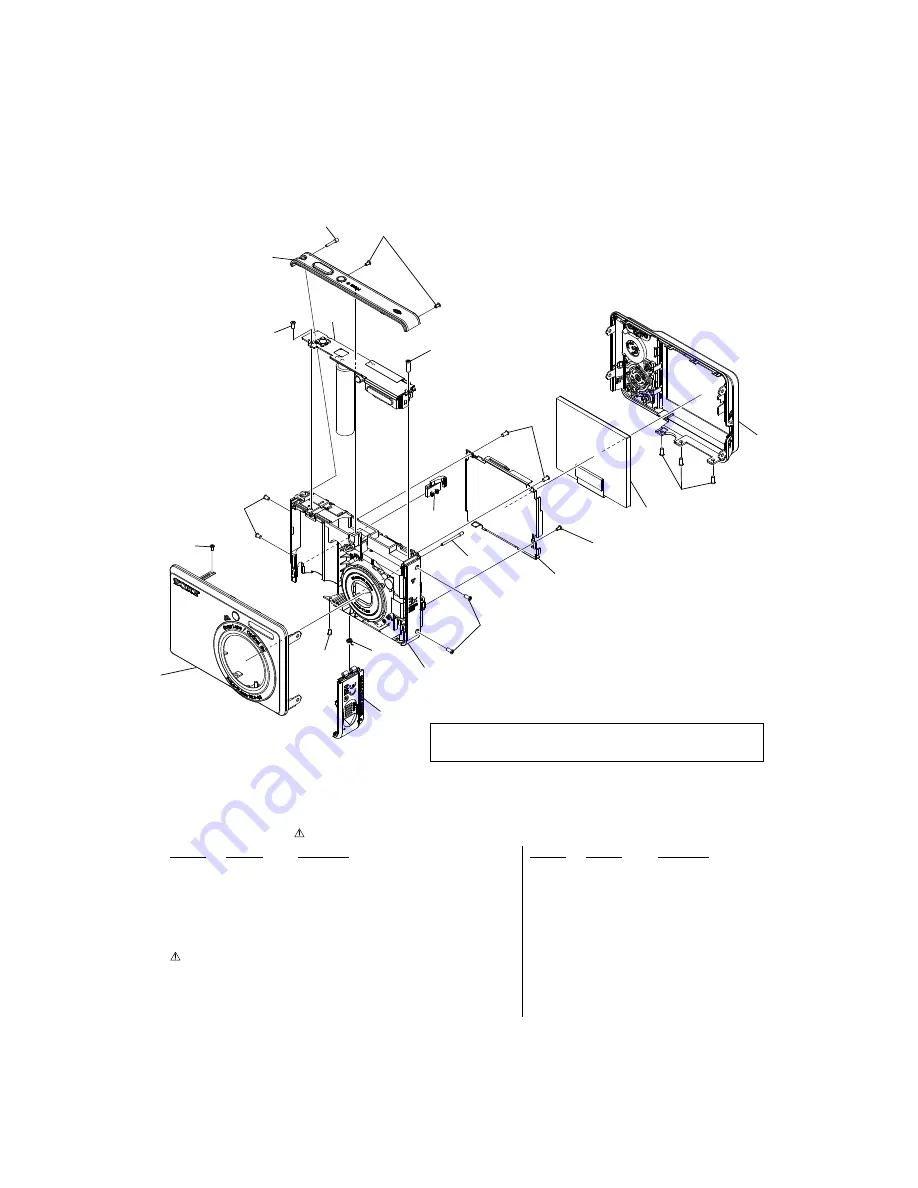
EXPLODED VIEWS

4-1-1.

OVERALL SECTION

Ref. No.

Part No.

Description

Ref. No.

Part No.

Description

1

X-2188-411-1 CABINET (FRONT) ASSY

2

X-2188-412-1 CABINET (REAR) ASSY

3

3-286-696-01 SHAFT, STRAP

4

3-286-697-01 BLOCK, RL

5

3-286-698-01 LCD

6

A-1444-049-A ST BLOCK ASSY

7

3-286-700-01 SHAFT, BT LID

8

3-286-701-01 LID, BT

9

3-286-702-01 SPRING, BT LID

10

3-286-703-01 LID, JACK

11

3-287-023-11 SCREW M1.7 X 2.7

12

3-287-026-01 SCREW TP1.4 X 2.5

13

3-287-028-01 SCREW TP1.7 X 3.5

14

3-287-027-01 SCREW TP1.7 X 4

15

3-287-025-01 SCREW TP1.4 X 3

16

3-287-032-01 SCREW TP1.7 X 6.5

17

3-296-920-01 SCREW TP1.4 X 3.5

18

3-296-921-01 SCREW TP1.4 X 4

19

3-299-366-01 SCREW TP1.7 X 3.5

•  Refer to cover for mark    .

ns: not supplied

Note : The adjustment is not required after replacing the LCD

1

2

3

4

5

6

7

9

Main Frame Block
(See Page 4-2)

ns

11

17

12

18

13

14

15

8

16

10

19

15

(Note)

Summary of Contents for DSC S730 - Cyber-shot Digital Camera

Page 1: ...ian Model AEP Model UK Model E Model Australian Model Hong Kong Model Chinese Model Korea Model Tourist Model The components identified by mark or dotted line with mark are critical for safety Replace only with part num ber specified Les composants identifiés par une marque sont critiques pour la sécurité Ne les remplacer que par une pièce portant le numéro spécifié DSC S730 In case of the lens bl...

Page 2: ...I Compatible PictBridge Compatible System Image device 7 20 mm 1 2 5 type color CCD Primary color filter Total pixel number of camera Approx 7 410 000 pixels Effective pixel number of camera Approx 7 201 000 pixels Lens 3 zoom lens f 5 8 17 4 mm 35 105 mm when converted to a 35 mm still camera F2 8 W 4 8 T Exposure control Automatic exposure Scene Selection 7 modes White balance Automatic Daylight...

Page 3: ... Repairing Keep the temperature of the soldering iron around 270 C during repairing Do not touch the soldering iron on the same conductor of the circuit board within 3 times Be careful not to apply force on the conductor when soldering or unsoldering Unleaded solder Boards requiring use of unleaded solder are printed with the lead free mark LF indicating the solder contains no lead Caution Some pr...

Page 4: ...1 1 1 2 Method for Copying or Erasing the Data in Internal Memory 1 1 2 DISASSEMBLY 2 1 Disassembly 2 1 3 BLOCK DIAGRAM 3 1 Overall Block Diagram 3 1 4 REPAIR PARTS LIST 4 1 Exploded Views 4 1 4 1 1 Overall Section 4 1 4 1 2 Main Frame Block 4 2 4 2 Accessories 4 3 Section Title Page ...

Page 5: ...ress z The message All data in internal memory will be copied Ready appears 3 Select OK with v then press z Copying starts To cancel copying Select Cancel in step 2 or 3 then press z Use batteries with enough power remaining If you attempt to copy image files using batteries with little remaining charge the batteries may run out causing copying to fail or possibly corrupting the data You cannot se...

Page 6: ...X 4 3 1 2 1 CABINET FRONT ASSY 2 SCREW TP 1 4 X 2 5 3 SCREW TP 1 4 X 3 1 2 3 1 BT LID SHAFT To 2 2 Page 2 BT LID 3 BT LID SPRING Note When CABINET FRONT ASSY is removed the plate will bends if CABINET FRONT ASSY is inclined too much Please remove CABINET FRONT ASSY as in parallel as possible plate 2 1 DISASSEMBLY 2 DISASSEMBLY The following flow chart shows the disassembly procedure ...

Page 7: ...parent seal removed when discharged 3 1 2 1 STRAP SHAFT From 2 1 Page 2 RL BLOCK 3 SCREW TP 1 4 X 3 1 3 1 ST BLOCK ASSY 2 SCREW TP 1 7 X 3 5 3 SCREW TP 1 7 X 6 5 1 2 3 1 SUPPORT JACK 2 MAIN MOUNT 3 SCREW TP 1 4 X 2 5 4 SCREW TP 1 7 X 3 5 4 1 2 3 5 4 1 JACK LID 2 MAIN FRAME 3 LENS BLOCK ASSY 4 LID 5 SCREW TP 1 4 X 3 2 ...

Page 8: ...PWR_CTRL 13 4V 2 5VD 1 8VD 3 3V 3 1VD 5VM VP DGND CCD_ON1 3 1 4 2 5 6 1 2 DSP DSP VSUB_Con1 AFERST VSUB_Con2 CCD 0 11 PXCLK SCLK SDATA CDS_EN VD TG_EN HD RAMD 0 15 RAMREF RAMA 0 14 RAMCLK_EN RAMLDQS RAMWE_N RAMCS_N RAMRAS RAMCAS RAMLDM RAMUDM LENS_EN STROBE_CHG SHUTTER_M0 SHUTTER_M1 LENS_SCLK LENS_SDATA LENS_PS USB_DET D D PWR_CTRL STROBE_TRG PWR_ON LCD 0 7 LCD_HD LCD_VD LCD_SDATA LCD_EN LCD_SCLK ...

Page 9: ...T 9 3 286 702 01 SPRING BT LID 10 3 286 703 01 LID JACK 11 3 287 023 11 SCREW M1 7 X 2 7 12 3 287 026 01 SCREW TP1 4 X 2 5 13 3 287 028 01 SCREW TP1 7 X 3 5 14 3 287 027 01 SCREW TP1 7 X 4 15 3 287 025 01 SCREW TP1 4 X 3 16 3 287 032 01 SCREW TP1 7 X 6 5 17 3 296 920 01 SCREW TP1 4 X 3 5 18 3 296 921 01 SCREW TP1 4 X 4 19 3 299 366 01 SCREW TP1 7 X 3 5 Refer to cover for mark ns not supplied Note ...

Page 10: ...3 5 105 3 286 704 01 FRAME MAIN 4 REPAIR PARTS LIST ns not supplied 101 105 102 102 103 104 104 Note 1 In case of the lens block assy or main board failure contact your local Sony service Headquarter for the measures Note 2 When separate lens block assy and main board for main frame replacement assemble original lens block assy and main board back after repaire Note 2 Note 1 ns ns Note 1 ns ...

Page 11: ...ANISH PORTUGUESE AEP E JE 3 281 198 41 GERMAN DUTCH AEP 3 281 198 51 TRADITIONAL CHINESE SIMPLIFIED CHINESE E HK JE 3 281 198 61 RUSSIAN UKRAINIAN AEP 3 281 198 71 ARABIC PERSIAN E 3 281 198 81 KOREAN KR JE 3 281 198 91 POLISH CZECH AEP 3 281 199 11 HUNGARIAN SLOVAK AEP 3 281 199 21 SWEDISH FINNISH AEP 3 281 199 31 NORWEGIAN DANISH AEP 3 281 199 41 THAI MALAYSIAN E 3 281 199 51 TURKISH GREEK AEP 3...

Page 12: ...MANUFACTURER KAMAYA ELECTRIC CO LTD TYPE FCC16162AD RATING 1 6A MANUFACTURER KAMAYA ELECTRIC CO LTD TYPE FCC10102AD RATING 1 0A MAIN BOARD Regarding Fuse F5 F3 F5 F3 DSC S730 ...

Page 13: ...DSC S730 Revision History Reverse Ver 1 0 Date 2007 11 History Official Release Contents S M Rev issued 985223911 pdf ...

Reviews: