


RB1G
CHASSIS
W900A/904A/905A
Troubleshooting
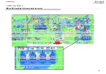
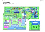
3-3-3. Main Board Power Off Checking (for Main SP Lch & Rch)
No
Checking Item
OK
NG
5
Check connectivity audio output path (only for BA2
and BM board):
L4601 (near to IC side) – CN4601 Pin1
L4602 (near to IC side) – CN4601 Pin2
L4603 (
t IC id )
CN4601 Pi 3
Must have good connection
(~0
Ω
)
Open circuit.
L4603 (near to IC side) – CN4601 Pin3
L4604 (near to IC side) – CN4601 Pin4
6
Check connectivity audio output path
(only for BKE and BKX board):
Must have good connection
(~0
Ω
)
Open circuit.
(
y
)
L4601 (near to IC side) – CN4601 Pin4
L4602 (near to IC side) – CN4601 Pin3
L4603 (near to IC side) – CN4601 Pin2
L4604 (near to IC side) – CN4601 Pin1
(
)
Size
B* Board Type
G* Board
Type
OTHERS JP
40”
BA2-S BA2-W
G1A
82
46”
BA2-S BA2-W
G1A
55”
BA2-S
BA2-W
G1B
Summary of Contents for BRAVIA KDL-55W900A
Page 2: ...SERVICE MANUAL COMMON SERVICE MANUAL COMMON RB1G CHASSIS Segment HG LCD TV LCD TV ...
Page 118: ...RB1G CHASSIS W900A 904A 905A Troubleshooting 3 4 RB1 Analog Signal Path 118 ...
Page 149: ...RB1G CHASSIS W900A 904A 905A Troubleshooting Troubleshooting Reference BA2S SIDE B IC2201 149 ...
Page 159: ...RB1G CHASSIS W900A 904A 905A Troubleshooting Troubleshooting Reference BA2S SIDE B IC2201 159 ...
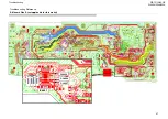
Page 232: ...RB1G CHASSIS W900A 904A 905A 5 2 Block Diagram Diagrams g 5 2 1 EUROPE 232 ...
Page 233: ...RB1G CHASSIS W900A 904A 905A 5 2 Block Diagram Diagrams 5 2 Block Diagram 5 2 2 JAPAN 233 ...
Page 234: ...RB1G CHASSIS W900A 904A 905A 5 2 Block Diagram Diagrams g 5 2 3 UC 234 ...
Page 236: ...RB1G CHASSIS W900A 904A 905A 5 2 Block Diagram Diagrams 5 2 Block Diagram 5 2 5 CHINA HK 236 ...
Page 237: ...RB1G CHASSIS W900A 904A 905A 5 2 Bl k Di Diagrams 5 2 Block Diagram 5 2 6 TAIWAN COL 237 ...
Page 238: ...RB1G CHASSIS W900A 904A 905A 2 Diagrams 5 2 Block Diagram 5 2 7 PAN ASIA 238 ...